Datasheet 搜索 > 放大器、缓冲器 > ADI(亚德诺) > AD823AR 数据手册 > AD823AR 数据手册 1/20 页

 器件3D模型
¥ 7.268
AD823AR 数据手册 - ADI(亚德诺)
制造商:
ADI(亚德诺)
分类:
放大器、缓冲器
封装:
SOIC-8
描述:
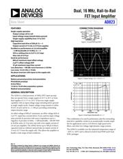
双通道, 16 MHz的轨到轨FET输入放大器 Dual, 16 MHz, Rail-to-Rail FET Input Amplifier
Pictures:
3D模型
符号图
焊盘图
引脚图
产品图
页面导航:
导航目录
AD823AR数据手册
Page:
of 20 Go
若手册格式错乱,请下载阅览PDF原文件
Dual, 16 MHz, Rail-to-Rail
FET Input Amplifier
Data Sheet
AD823
Rev. E
Information furnished by Analog Devices is believed to be accurate and reliable. However, no
responsibility is assumed by Analog Devices for its use, nor for any infringements of patents or other
rights
of third parties that may result from its use. Specifications subject to change without notice. No
license is granted by implication or otherwise under any patent or patent rights of Analog Devices.
Trademarks and registered trademarks are the property of their respective owners.
One Technology Way, P.O. Box 9106, Norwood, MA 02062-9106, U.S.A.
Tel: 781.329.4700 www.analog.com
Fax: 781.461.3113 ©1995–2011 Analog Devices, Inc. All rights reserved.
FEATURES
Single-supply operation
Output swings rail-to-rail
Input voltage range extends below ground
Single-supply capability from 3 V to 36 V
High load drive
Capacitive load drive of 500 pF, G = +1
Output current of 15 mA, 0.5 V from supplies
Excellent ac performance on 2.6 mA/amplifier
−3 dB bandwidth of 16 MHz, G = +1
350 ns settling time to 0.01% (2 V step)
Slew rate of 22 V/µs
Good dc performance
800 µV maximum input offset voltage
2 µV/°C offset voltage drift
25 pA maximum input bias current
Low distortion: −108 dBc worst harmonic @ 20 kHz
Low noise: 16 nV/√Hz @ 10 kHz
No phase inversion with inputs to the supply rails
APPLICATIONS
Battery-powered precision instrumentation
Photodiode preamps
Active filters
12-bit to 16-bit data acquisition systems
Medical instrumentation
GENERAL DESCRIPTION
The AD823 is a dual precision, 16 MHz, JFET input op amp
that can operate from a single supply of 3.0 V to 36 V or from
dual supplies of ±1.5 V to ±18 V. It has true single-supply
capability with an input voltage range extending below ground
in single-supply mode. Output voltage swing extends to within
50 mV of each rail for I
OUT
≤ 100 µA, providing outstanding
output dynamic range.
An offset voltage of 800 µV maximum, an offset voltage drift of
2 µV/°C, input bias currents below 25 pA, and low input voltage
noise provide dc precision with source impedances up to a
Gigaohm. It provides 16 MHz, −3 dB bandwidth, −108 dB THD
@ 20 kHz, and a 22 V/µs slew rate with a low supply current of
2.6 mA per amplifier. The AD823 drives up to 500 pF of direct
capacitive load as a follower and provides an output current of
15 mA, 0.5 V from the supply rails. This allows the amplifier to
handle a wide range of load conditions.
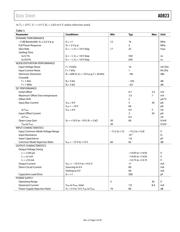
CONNECTION DIAGRAM
AD823
OUT1
+IN2
–IN2
OUT2
+V
S
–IN1
+IN1
–V
S
1
2
3
4
8
7
6
5
00901-001
Figure 1. 8-Lead PDIP and SOIC
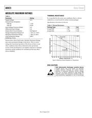
3V
GND
00901-002
R
L
= 100kΩ
C
L
= 50pF
+V
S
= +3V
G = +1
500mV 200µs
Figure 2. Output Swing, +V
S
= +3 V, G = +1
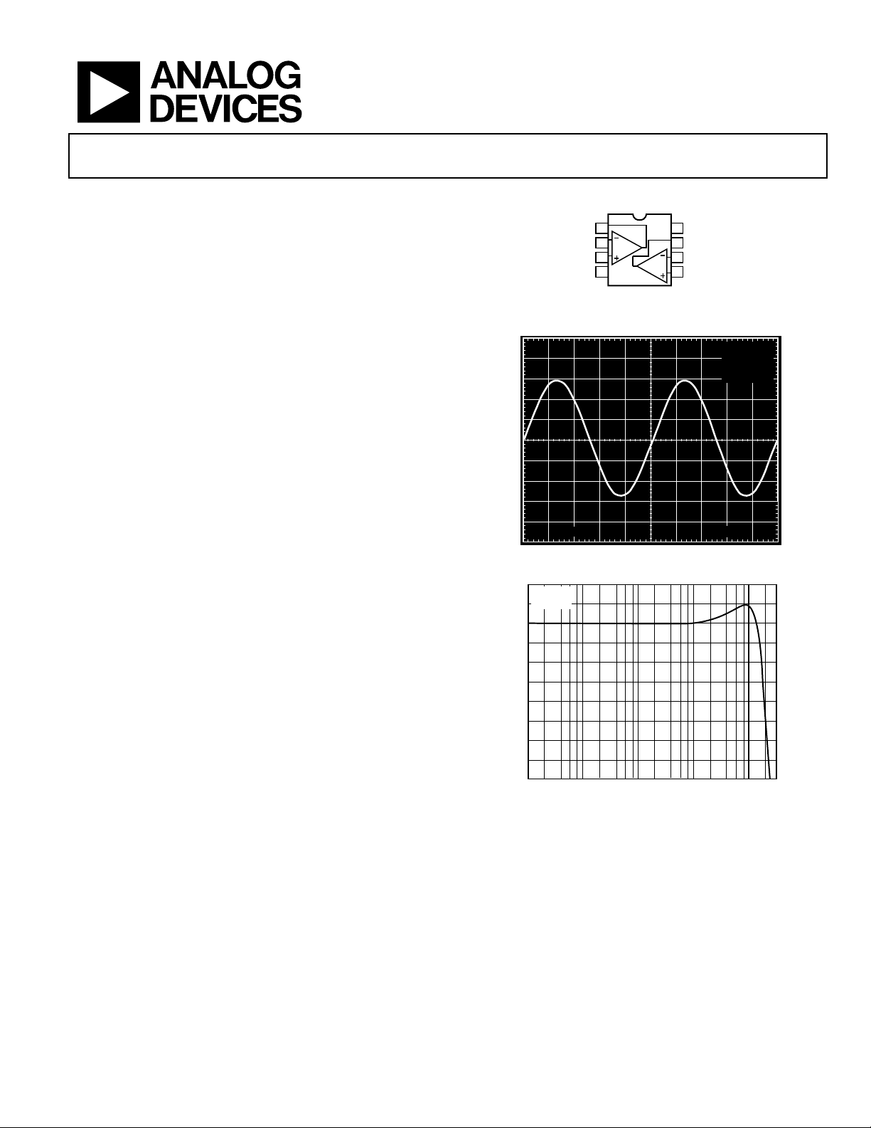
FREQUENCY (Hz)
–8
OUTPUT (dB)
1k
–6
–7
2
1
10k 100k 1M
+V
S
= +5V
G = +1
–5
–4
–3
–2
–1
0
10M
00901-003
Figure 3. Small Signal Bandwidth, G = +1
This combination of ac and dc performance, plus the outstanding
load drive capability, results in an exceptionally versatile ampli-
fier for applications such as A/D drivers, high speed active
filters, and other low voltage, high dynamic range systems.
The AD823 is available over the industrial temperature range of
−40°C to +85°C and is offered in both 8-lead PDIP and 8-lead
SOIC packages.
器件 Datasheet 文档搜索
AiEMA 数据库涵盖高达 72,405,303 个元件的数据手册,每天更新 5,000 多个 PDF 文件
