Datasheet 搜索 > 射频检测器 > ADI(亚德诺) > AD8314ACP-WP 数据手册 > AD8314ACP-WP 数据手册 1/20 页

¥ 45.328
AD8314ACP-WP 数据手册 - ADI(亚德诺)
制造商:
ADI(亚德诺)
分类:
射频检测器
封装:
LFCSP
描述:
100 MHz至2.7 GHz的, 45分贝RF检测器/控制器 100 MHz to 2.7 GHz, 45 dB RF Detector/Controller
Pictures:
3D模型
符号图
焊盘图
引脚图
产品图
页面导航:
引脚图在P5Hot
原理图在P1P10P18
封装尺寸在P20
型号编码规则在P18P20
封装信息在P20
功能描述在P1P5
技术参数、封装参数在P1P3P4P11
应用领域在P1P3P10P12
电气规格在P6
导航目录
AD8314ACP-WP数据手册
Page:
of 20 Go
若手册格式错乱,请下载阅览PDF原文件
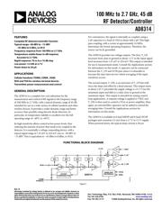
100 MHz to 2.7 GHz, 45 dB
RF Detector/Controller
AD8314
Rev. B
Information furnished by Analog Devices is believed to be accurate and reliable. However, no
responsibility is assumed by Analog Devices for its use, nor for any infringements of patents or other
rights of third parties that may result from its use. Specifications subject to change without notice. No
license is granted by implication or otherwise under any patent or patent rights of Analog Devices.
Trademarks and registered trademarks are the property of their respective owners.
One Technology Way, P.O. Box 9106, Norwood, MA 02062-9106, U.S.A.
Tel: 781.329.4700 www.analog.com
Fax: 781.461.3113 ©2006 Analog Devices, Inc. All rights reserved.
FEATURES
Complete RF detector/controller function
Typical range:−58 dBV to −13 dBV
−45 dBm to 0 dBm, re 50 Ω
Frequency response from 100 MHz to 2.7 GHz
Temperature-stable linear-in-dB response
Accurate to 2.7 GHz
Rapid response: 70 ns to a 10 dB step
Low power: 12 mW at 2.7 V
Power down to 20 μA
APPLICATIONS
Cellular handsets (TDMA, CDMA , GSM)
RSSI and TSSI for wireless terminal devices
Transmitter power measurement and control
GENERAL DESCRIPTION
The AD8314 is a complete low cost subsystem for the
measurement and control of RF signals in the frequency range
of 100 MHz to 2.7 GHz, with a typical dynamic range of 45 dB,
intended for use in a wide variety of cellular handsets and other
wireless devices. It provides a wider dynamic range and better
accuracy than possible using discrete diode detectors. In
particular, its temperature stability is excellent over the full
operating range of −40°C to +85°C.
Its high sensitivity allows control at low power levels, thus
reducing the amount of power that needs to be coupled to the
detector. It is essentially a voltage-responding device, with a
typical signal range of 1.25 mV to 224 mV rms or –58 dBV to
−13 dBV. This is equivalent to −45 dBm to 0 dBm, re 50 Ω.
For convenience, the signal is internally ac-coupled, using a
5 pF capacitor to a load of 3 kΩ in shunt with 2 pF. This high-
pass coupling, with a corner at approximately 16 MHz,
determines the lowest operating frequency. Therefore, the
source can be dc grounded.
The AD8314 provides two voltage outputs. The first, V_UP,
increases from close to ground to about 1.2 V as the input signal
level increases from 1.25 mV to 224 mV. This output is intended
for use in measurement mode. Consult the
Applications section
for information on this mode. A capacitor can be connected
between the V_UP and FLTR pins when it is desirable to
increase the time interval over which averaging of the input
waveform occurs.
The second output, V_DN, is an inversion of V_UP but with
twice the slope and offset by a fixed amount. This output starts
at about 2.25 V (provided the supply voltage is ≥3.3 V) for the
minimum input and falls to a value close to ground at the
maximum input. This output is intended for analog control
loop applications. A setpoint voltage is applied to VSET, and
V_DN is then used to control a VGA or power amplifier. Here
again, an external filter capacitor can be added to extend the
averaging time. Consult the
Applications section for
information on this mode.
The AD8314 is available in 8-lead MSOP and 8-lead LFCSP
packages and consumes 4.5 mA from a 2.7 V to 5.5 V supply.
When powered down, the typical sleep current is 20 µA.
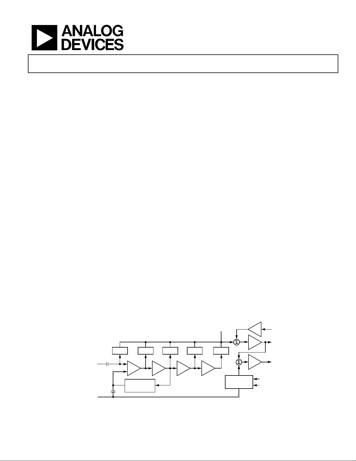
FUNCTIONAL BLOCK DIAGRAM
10dB
OFFSET
COMPENSATION
V-I
I-V
RFIN
COMM
(
PADDLE)
VPOS
X2
ENBL
V_DN
V_UP
VSET
FLTR
AD8314
10dB10dB 10dB
BAND GAP
REFERENCE
DETDET
+
–
–
+
DETDETDET
01086-001
Figure 1.
器件 Datasheet 文档搜索
AiEMA 数据库涵盖高达 72,405,303 个元件的数据手册,每天更新 5,000 多个 PDF 文件
