Datasheet 搜索 > ADI(亚德诺) > AD8502 数据手册 > AD8502 数据手册 6/24 页


¥ 0
AD8502 数据手册 - ADI(亚德诺)
制造商:
ADI(亚德诺)
Pictures:
3D模型
符号图
焊盘图
引脚图
产品图
页面导航:
导航目录
AD8502数据手册
Page:
of 24 Go
若手册格式错乱,请下载阅览PDF原文件
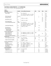
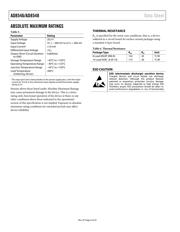
AD8546/AD8548 Data Sheet
Rev. B | Page 6 of 24
ABSOLUTE MAXIMUM RATINGS
Table 5.
Parameter Rating
Supply Voltage 20.5 V
Input Voltage
(V−) − 300 mV to (V+) + 300 mV
Input Current
1
±10 mA
Differential Input Voltage ±V
SY
Output Short-Circuit Duration
to GND
Indefinite
Storage Temperature Range −65°C to +150°C
Operating Temperature Range
−40°C to +125°C
Junction Temperature Range −65°C to +150°C
Lead Temperature
(Soldering, 60 sec)
300°C
1
The input pins have clamp diodes to the power supply pins. Limit the input
current to 10 mA or less whenever input signals exceed the power supply
rail by 0.3 V.
Stresses above those listed under Absolute Maximum Ratings
may cause permanent damage to the device. This is a stress
rating only; functional operation of the device at these or any
other conditions above those indicated in the operational
section of this specification is not implied. Exposure to absolute
maximum rating conditions for extended periods may affect
device reliability.
THERMAL RESISTANCE
θ
JA
is specified for the worst-case conditions, that is, a device
soldered in a circuit board for surface-mount packages using
a standard 4-layer board.
Table 6. Thermal Resistance
Package Type
θ
JA
θ
JC
Unit
8-Lead MSOP (RM-8) 142 45 °C/W
14-Lead SOIC_N (R-14)
115
36
°C/W
ESD CAUTION
器件 Datasheet 文档搜索
AiEMA 数据库涵盖高达 72,405,303 个元件的数据手册,每天更新 5,000 多个 PDF 文件
