Datasheet 搜索 > AD转换器 > ADI(亚德诺) > AD9236BCPRL7-80 数据手册 > AD9236BCPRL7-80 数据手册 1/36 页

¥ 0
AD9236BCPRL7-80 数据手册 - ADI(亚德诺)
制造商:
ADI(亚德诺)
分类:
AD转换器
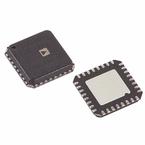
封装:
VFQFN-32
描述:
12位, 80 MSPS , 3 V A / D转换器 12-Bit, 80 MSPS, 3 V A/D Converter
Pictures:
3D模型
符号图
焊盘图
引脚图
产品图
页面导航:
引脚图在P9Hot
原理图在P1P20P21P22P23P27P28P29
封装尺寸在P33
型号编码规则在P34
功能描述在P1P9
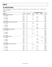
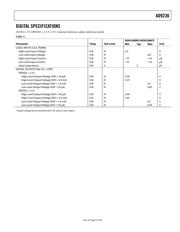
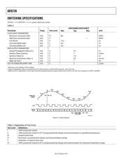
技术参数、封装参数在P1P3P4P5P6P7
应用领域在P1P16
电气规格在P11P16
导航目录
AD9236BCPRL7-80数据手册
Page:
of 36 Go
若手册格式错乱,请下载阅览PDF原文件
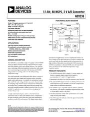
12-Bit, 80 MSPS, 3 V A/D Converter
AD9236
Rev. B
Information furnished by Analog Devices is believed to be accurate and reliable. However, no
responsibility is assumed by Analog Devices for its use, nor for any infringements of patents or other
rights of third parties that may result from its use. Specifications subject to change without notice. No
license is granted by implication or otherwise under any patent or patent rights of Analog Devices.
Trademarks and registered trademarks are the property of their respective owners.
One Technology Way, P.O. Box 9106, Norwood, MA 02062-9106, U.S.A.
Tel: 781.329.4700 www.analog.com
Fax: 781.461.3113 © 2006 Analog Devices, Inc. All rights reserved.
FEATURES
Single 3 V supply operation (2.7 V to 3.6 V)
SNR = 70.4 dBc to Nyquist
SFDR = 87.8 dBc to Nyquist
Low power: 366 mW
Differential input with 500 MHz bandwidth
On-chip reference and sample-and-hold
DNL = ±0.4 LSB
Flexible analog input: 1 V p-p to 2 V p-p range
Offset binary or twos complement data format
Clock duty cycle stabilizer
APPLICATIONS
High end medical imaging equipment
IF sampling in communications receivers
WCDMA, CDMA-One, CDMA-2000
Battery-powered instruments
Hand-held scopemeters
Low cost digital oscilloscopes
DTV subsystems
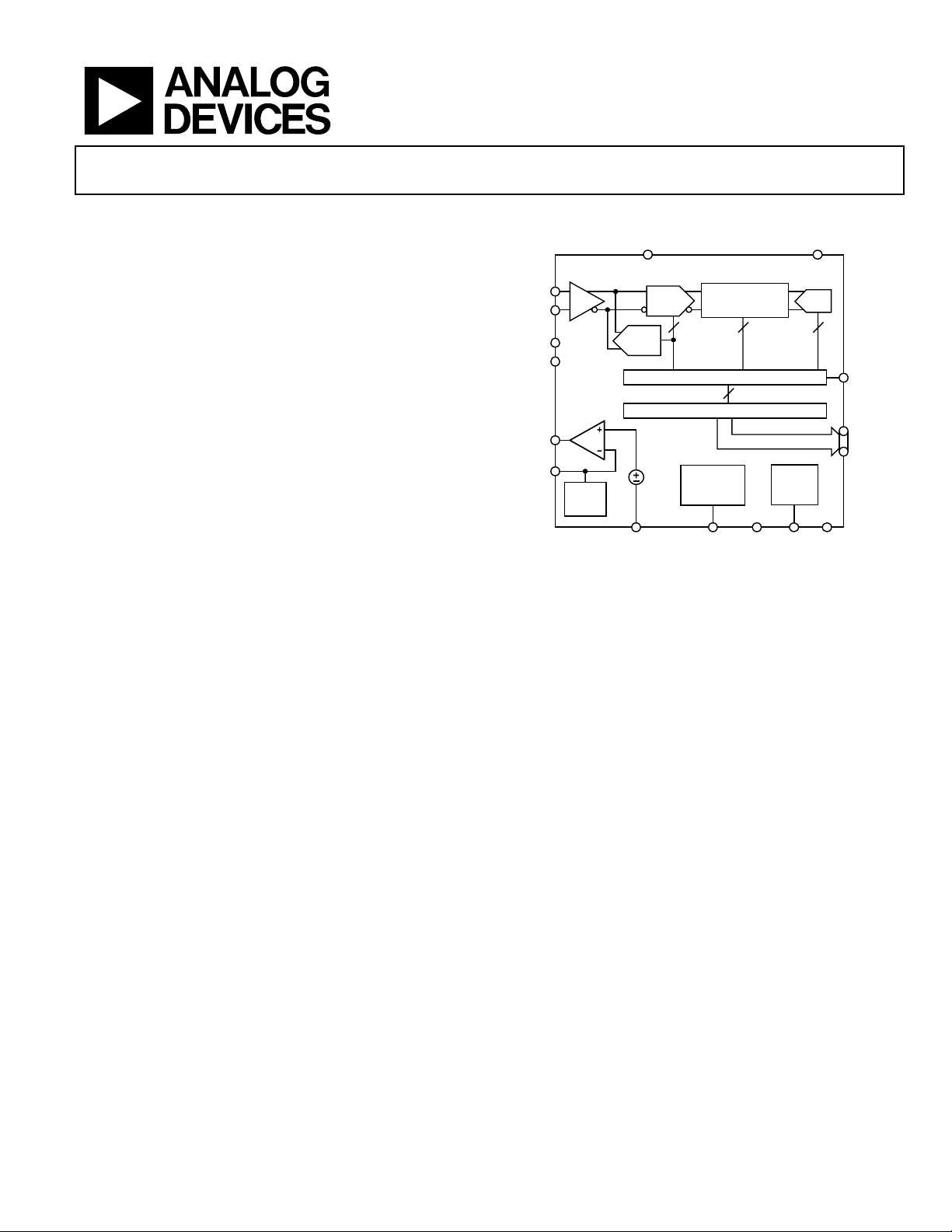
GENERAL DESCRIPTION
The AD9236 is a monolithic, single 3 V supply, 12-bit, 80 MSPS
analog-to-digital converter featuring a high performance sample-
and-hold amplifier (SHA) and voltage reference. The AD9236
uses a multistage differential pipelined architecture with output
error correction logic to provide 12-bit accuracy at 80 MSPS
and guarantee no missing codes over the full operating
temperature range.
The wide bandwidth, truly differential SHA allows a variety of
user-selectable input ranges and common modes, including
single-ended applications. It is suitable for multiplexed systems
that switch full-scale voltage levels in successive channels and
for sampling single-channel inputs at frequencies well beyond
the Nyquist rate. Combined with power and cost savings over
previously available analog-to-digital converters, the AD9236 is
suitable for applications in communications, imaging, and
medical ultrasound.
A single-ended clock input is used to control all internal
conversion cycles. A duty cycle stabilizer (DCS) compensates
for wide variations in the clock duty cycle while maintaining
excellent overall ADC performance. The digital output data is
FUNCTIONAL BLOCK DIAGRAM
03066-0-001
DRVDDAVDD
AGND
0.5V
CLK PDWN MODE DGND
OTR
VIN+
VIN–
REFT
REFB
AD9236
VREF
SENSE
SHA
A/D
MDAC1
4
16
12
3
A/D
8-STAGE
1 1/2-BIT PIPELINE
REF
SELECT
CLOCK
DUTY CYCLE
STABILIZER
MODE
SELECT
CORRECTION LOGIC
OUTPUT BUFFERS
D11 (MSB)
D0 (LSB)
Figure 1.
presented in straight binary or twos complement formats. An
out-of-range (OTR) signal indicates an overflow condition that
can be used with the most significant bit to determine low or
high overflow. Fabricated on an advanced CMOS process, the
AD9236 is available in a 28-lead TSSOP and a 32-lead LFCSP
and is specified over the industrial temperature range
(−40°C to +85°C).
PRODUCT HIGHLIGHTS
1. The AD9236 operates from a single 3 V power supply and
features a separate digital output driver supply to
accommodate 2.5 V and 3.3 V logic families.
2. Operating at 80 MSPS, the AD9236 consumes a low 366 mW.
3. The patented SHA input maintains excellent performance for
input frequencies up to 100 MHz, and can be configured for
single-ended or differential operation.
4. The AD9236 is pin compatible with the AD9215, AD9235,
and AD9245. This allows a simplified migration from 10 bits
to 14 bits and 20 MSPS to 80 MSPS.
5. The DCS maintains overall ADC performance over a wide
range of clock pulse widths.
6. The OTR output bit indicates when the signal is beyond the
selected input range.
器件 Datasheet 文档搜索
AiEMA 数据库涵盖高达 72,405,303 个元件的数据手册,每天更新 5,000 多个 PDF 文件
