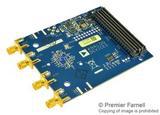
Datasheet 搜索 > 开发套件与开发板 > ADI(亚德诺) > AD9361/PCBZ 数据手册 > AD9361/PCBZ 数据手册 1/38 页

¥ 43079.94
AD9361/PCBZ 数据手册 - ADI(亚德诺)
制造商:
ADI(亚德诺)
分类:
开发套件与开发板
描述:
ANALOG DEVICES AD9361/PCBZ 评估板,AD9361
Pictures:
3D模型
符号图
焊盘图
引脚图
产品图
页面导航:
引脚图在P9P18Hot
原理图在P1
封装尺寸在P38
型号编码规则在P38
封装信息在P38
焊接温度在P17
功能描述在P1P9P18
技术参数、封装参数在P1P5P7P17
应用领域在P1P2
电气规格在P5P22
导航目录
AD9361/PCBZ数据手册
Page:
of 38 Go
若手册格式错乱,请下载阅览PDF原文件
RF Agile Transceiver
Data Sheet
AD9361
Rev. F Document Feedback
Information furnished by Analog Devices is believed to be accurate and reliable. However, no
responsibility is assumed by Analog Devices for its use, nor for any infringements of patents or other
rights of third parties that may result from its use. Specifications subject to change without notice. No
license is granted by implication or otherwise under any patent or patent rights of Analog Devices.
Trademarks and registered trademarks are the property of their respective owners.
One Technology Way, P.O. Box 9106, Norwood, MA 02062-9106, U.S.A.
Tel: 781.329.4700 ©2013–2016 Analog Devices, Inc. All rights reserved.
Technical Support www.analog.com
FEATURES
RF 2 × 2 transceiver with integrated 12-bit DACs and ADCs
TX band: 47 MHz to 6.0 GHz
RX band: 70 MHz to 6.0 GHz
Supports TDD and FDD operation
Tunable channel bandwidth: <200 kHz to 56 MHz
Dual receivers: 6 differential or 12 single-ended inputs
Superior receiver sensitivity with a noise figure of 2 dB at
800 MHz LO
RX gain control
Real-time monitor and control signals for manual gain
Independent automatic gain control
Dual transmitters: 4 differential outputs
Highly linear broadband transmitter
TX EVM: ≤−40 dB
TX noise: ≤−157 dBm/Hz noise floor
TX monitor: ≥66 dB dynamic range with 1 dB accuracy
Integrated fractional-N synthesizers
2.4 Hz maximum local oscillator (LO) step size
Multichip synchronization
CMOS/LVDS digital interface
APPLICATIONS
Point to point communication systems
Femtocell/picocell/microcell base stations
General-purpose radio systems
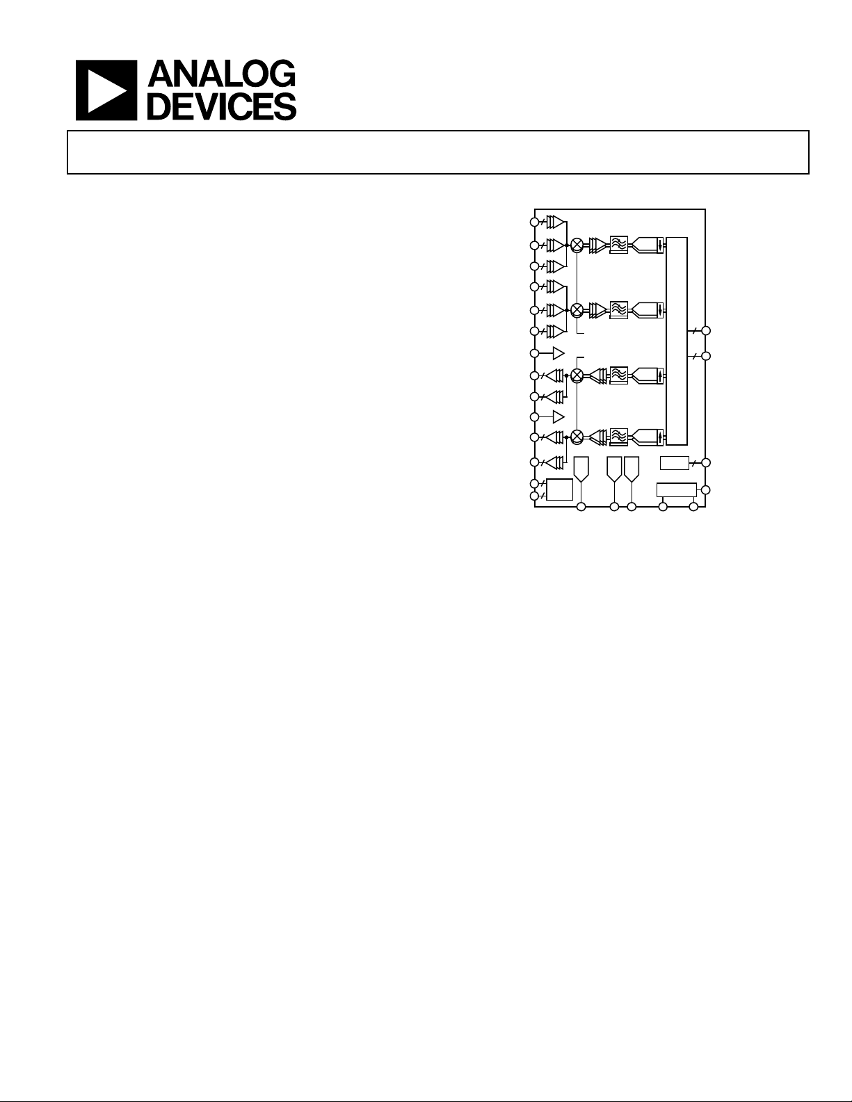
FUNCTIONAL BLOCK DIAGRAM
Figure 1.
GENERAL DESCRIPTION
The AD9361 is a high performance, highly integrated radio
frequency (RF) Agile Transceiver™ designed for use in 3G and
4G base station applications. Its programmability and wideband
capability make it ideal for a broad range of transceiver applications.
The device combines a RF front end with a flexible mixed-signal
baseband section and integrated frequency synthesizers, simplifying
design-in by providing a configurable digital interface to a
processor. The AD9361 receiver LO operates from 70 MHz to
6.0 GHz and the transmitter LO operates from 47 MHz to 6.0 GHz
range, covering most licensed and unlicensed bands. Channel
bandwidths from less than 200 kHz to 56 MHz are supported.
The two independent direct conversion receivers have state-of-the-
art noise figure and linearity. Each receive (RX) subsystem includes
independent automatic gain control (AGC), dc offset correction,
quadrature correction, and digital filtering, thereby eliminating
the need for these functions in the digital baseband. The AD9361
also has flexible manual gain modes that can be externally
controlled. Two high dynamic range analog-to-digital converters
(ADCs) per channel digitize the received I and Q signals and pass
them through configurable decimation filters and 128-tap finite
impulse response (FIR) filters to produce a 12-bit output signal at
the appropriate sample rate.
The transmitters use a direct conversion architecture that achieves
high modulation accuracy with ultralow noise. This transmitter
design produces a best in class TX error vector magnitude (EVM)
of <−40 dB, allowing significant system margin for the external
power amplifier (PA) selection. The on-board transmit (TX)
power monitor can be used as a power detector, enabling highly
accurate TX power measurements.
The fully integrated phase-locked loops (PLLs) provide low
power fractional-N frequency synthesis for all receive and
transmit channels. Channel isolation, demanded by frequency
division duplex (FDD) systems, is integrated into the design.
All VCO and loop filter components are integrated.
The core of the AD9361 can be powered directly from a 1.3 V
regulator. The IC is controlled via a standard 4-wire serial port
and four real-time input/output control pins. Comprehensive
power-down modes are included to minimize power consumption
during normal use. The AD9361 is packaged in a 10 mm × 10 mm,
144-ball chip scale package ball grid array (CSP_BGA).
AD9361
RX1B_P,
RX1B_N
P1_[D11:D0]/
RX_[D5:D0]
P0_[D11:D0]/
TX_[D5:D0]
RADIO
SWITCHING
NOTES
1. SPI, CTRL, P0_[D11:D0]/TX_[D5:D0], P1_[D11:D0]/RX_[D5:D0],
AND RADIO SWITCHING CONTAIN MULTIPLE PINS.
RX1A_P,
RX1A_N
RX1C_P,
RX1C_N
RX2B_P,
RX2B_N
RX2A_P,
RX2A_N
RX2C_P,
RX2C_N
TX_MON1
DATA INTERFACE
RX LO
TX LO
TX1A_P,
TX1A_N
TX1B_P,
TX1B_N
TX_MON2
TX2A_P,
TX2A_N
TX2B_P,
TX2B_N
CTRL
AUXDACx XTALP XTALNAUXADC
CTRL
SPI
DAC
DAC
GPO
PLLs
DAC
ADC
CLK_OUT
DAC
ADC
ADC
10453-001
器件 Datasheet 文档搜索
AiEMA 数据库涵盖高达 72,405,303 个元件的数据手册,每天更新 5,000 多个 PDF 文件
