Datasheet 搜索 > ADI(亚德诺) > AD9364 数据手册 > AD9364 数据手册 3/33 页


¥ 0
AD9364 数据手册 - ADI(亚德诺)
制造商:
ADI(亚德诺)
Pictures:
3D模型
符号图
焊盘图
引脚图
产品图
页面导航:
引脚图在P8P12Hot
原理图在P1
封装尺寸在P32
型号编码规则在P32
封装信息在P32
焊接温度在P11
功能描述在P1P8P12
技术参数、封装参数在P1P4P6P11
应用领域在P1P2
电气规格在P4P16

导航目录
AD9364数据手册
Page:
of 33 Go
若手册格式错乱,请下载阅览PDF原文件

AD9364 Data Sheet
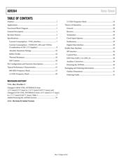
TABLE OF CONTENTS
Features .............................................................................................. 1
Applications ....................................................................................... 1
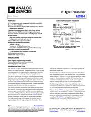
Functional Block Diagram .............................................................. 1
General Description ......................................................................... 1
Revision History ............................................................................... 2
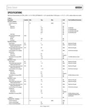
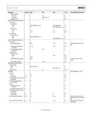
Specifications ..................................................................................... 3
Current Consumption—VDD_Interface .................................. 7
Current Consumption—VDDD1P3_DIG and VDDAx
(Combination of All 1.3 V Supplies) ......................................... 8
Absolute Maximum Ratings ..................................................... 10
Reflow Profile .............................................................................. 10
Thermal Resistance .................................................................... 10
ESD Caution ................................................................................ 10
Pin Configuration and Function Descriptions ........................... 11
Typical Performance Characteristics ........................................... 15
800 MHz Frequency Band ......................................................... 15
2.4 GHz Frequency Band .......................................................... 20
5.5 GHz Frequency Band .......................................................... 24
Theory of Operation ...................................................................... 28
General......................................................................................... 28
Receiver........................................................................................ 28
Transmitter .................................................................................. 28
Clock Input Options .................................................................. 28
Synthesizers ................................................................................. 29
Digital Data Interface................................................................. 29
Enable State Machine ..................................................................... 29
SPI Interface ................................................................................ 30
Control Pins ................................................................................ 30
GPO Pins (GPO_3 to GPO_0) ................................................. 30
Auxiliary Converters .................................................................. 30
Powering the AD9364 ................................................................ 30
Packaging and Ordering Information ......................................... 31
Outline Dimensions ................................................................... 31
Ordering Guide .......................................................................... 31
REVISION HISTORY
7/14—Rev. B to Rev. C
Changed CMOS VDD_INTERFACE from
1.2 V (min)/2.5 V (max) to 1.14 V (min)/2.625 V (max); and
Changed LVDS VDD_INTERFACE from 1.8 V (min)/2.5 V (max)
to 1.71 V (min)/2.625 V (max); Table 1......................................... 7
Added Powering the AD9364 Section ......................................... 30
2/14—Revision B: Initial Version
Rev. C | Page 2 of 32
器件 Datasheet 文档搜索
AiEMA 数据库涵盖高达 72,405,303 个元件的数据手册,每天更新 5,000 多个 PDF 文件
