Datasheet 搜索 > ADI(亚德诺) > AD9520-3 数据手册 > AD9520-3 数据手册 34/84 页


¥ 0
AD9520-3 数据手册 - ADI(亚德诺)
制造商:
ADI(亚德诺)
描述:
12 LVPECL / 24 CMOS输出时钟发生器,集成2 GHz的VCO 12 LVPECL/24 CMOS Output Clock Generator with Integrated 2 GHz VCO
Pictures:
3D模型
符号图
焊盘图
引脚图
产品图
页面导航:

导航目录
AD9520-3数据手册
Page:
of 84 Go
若手册格式错乱,请下载阅览PDF原文件
AD9520-3
Rev. 0 | Page 34 of 84
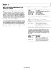
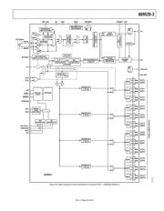
Phase-Locked Loop (PLL)
PROGRAMMABLE
N DELAY
REFIN
CLK
CLK
REF1
REF2
BUF
STATUS
STATUS
R
DIVIDER
CLOCK
DOUBLER
STATUS
PROGRAMMABLE
R DELAY
REFERENCE
SWITCHOVER
REF_SEL CPRSET
V
CP
V
S GND RSET
DISTRIBUTION
REFERENCE
REFMON
CP
STATUS
LD
P, P + 1
PRESCALER
A/B
COUNTERS
N DIVIDER
BYPASS
LF
LOW DROPOUT
REGULATOR (LDO)
PHASE
FREQUENCY
DETECTOR
LOCK
DETECT
CHARGE
PUMP
PLL
REFERENCE
HOLD
01
DIVIDE BY 1,
2, 3, 4, 5, OR 6
ZERO DELAY BLOCK
FROM CHANNEL
DIVIDER 0
VS_DRV
OPTIONAL
REFIN
0
7216-064
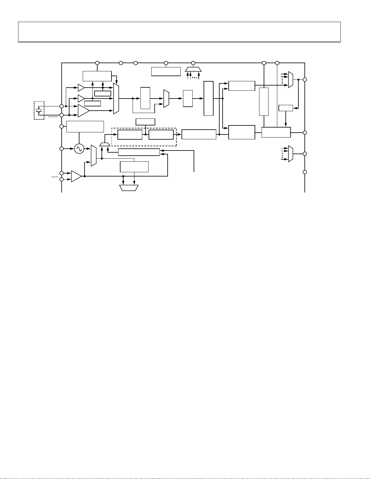
Figure 40. PLL Functional Block Diagram
The AD9520 includes an on-chip PLL with an on-chip VCO.
The PLL blocks can be used either with the on-chip VCO to
create a complete phase-locked loop or with an external VCO
or VCXO. The PLL requires an external loop filter, which
usually consists of a small number of capacitors and resistors.
The configuration and components of the loop filter help to
establish the loop bandwidth and stability of the operating PLL.
The AD9520 PLL is useful for generating clock frequencies
from a supplied reference frequency. This includes conversion
of reference frequencies to much higher frequencies for subsequent
division and distribution. In addition, the PLL can be used to
clean up jitter and phase noise on a noisy reference. The exact
choice of PLL parameters and loop dynamics is application
specific. The flexibility and depth of the AD9520 PLL allow the
part to be tailored to function in many different applications
and signal environments.
Configuration of the PLL
The AD9520 allows flexible configuration of the PLL,
accommodating various reference frequencies, PFD comparison
frequencies, VCO frequencies, internal or external VCO/VCXO,
and loop dynamics. This is accomplished by the various settings
for the R divider, the N divider, the PFD polarity (only applicable to
external VCO/VCXO), the antibacklash pulse width, the charge
pump current, the selection of internal VCO or external VCO/
VCXO, and the loop bandwidth. These are managed through
programmable register settings (see Table 49 and Table 53) and
by the design of the external loop filter.
Successful PLL operation and satisfactory PLL loop performance
are highly dependent upon proper configuration of the PLL
settings, and the design of the external loop filter is crucial to
the proper operation of the PLL.
ADIsimCLK™ is a free program that can help with the design
and exploration of the capabilities and features of the AD9520,
including the design of the PLL loop filter. The AD9516 model
found in ADIsimCLK Version 1.2 can also be used for modeling
the AD9520 loop filter. It is available at
www.analog.com/clocks.
Phase Frequency Detector (PFD)
The PFD takes inputs from the R divider and the N divider and
produces an output proportional to the phase and frequency
difference between them. The PFD includes a programmable
delay element that controls the width of the antibacklash pulse.
This pulse ensures that there is no dead zone in the PFD
transfer function and minimizes phase noise and reference
spurs. The antibacklash pulse width is set by 0x017[1:0].
An important limit to keep in mind is the maximum frequency
allowed into the PFD. The maximum input frequency into the
PFD is a function of the antibacklash pulse setting, as specified
in the Phase/Frequency Detector (PFD) parameter in Table 2.
器件 Datasheet 文档搜索
AiEMA 数据库涵盖高达 72,405,303 个元件的数据手册,每天更新 5,000 多个 PDF 文件
