Datasheet 搜索 > DA转换器 > ADI(亚德诺) > AD9714BCPZ 数据手册 > AD9714BCPZ 数据手册 12/80 页
 器件3D模型
¥ 4.768
AD9714BCPZ 数据手册 - ADI(亚德诺)
制造商:
ADI(亚德诺)
分类:
DA转换器
封装:
LFCSP-40
描述:
ANALOG DEVICES AD9714BCPZ 数模转换器, 双路, 8 bit, 串行, 1.7V 至 3.5V, LFCSP, 40 引脚
Pictures:
3D模型
符号图
焊盘图
引脚图
产品图
页面导航:
引脚图在P10P12P14P16P33P79Hot
典型应用电路图在P49
原理图在P4P32P53
封装尺寸在P79
型号编码规则在P79
功能描述在P1P10P12P14P16P79
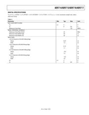
技术参数、封装参数在P1P5P7P8P9
应用领域在P1P46P48
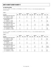
电气规格在P18
导航目录
AD9714BCPZ数据手册
Page:
of 80 Go
若手册格式错乱,请下载阅览PDF原文件
AD9714/AD9715/AD9716/AD9717
Rev. A | Page 12 of 80
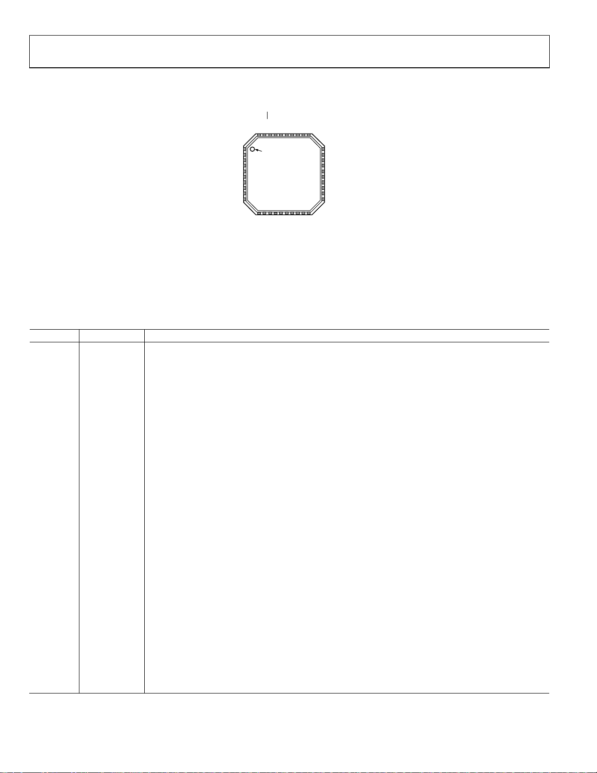
07265-067
PIN 1
INDICATOR
1DB7
2DB6
3DB5
4DB4
5DVDDIO
6DVSS
7DVDD
8DB3
9DB2
10DB1
23 QOUTP
24 RLQP
25 AVSS
26 AVDD
27 RLIP
28 IOUTP
29 IOUTN
30 RLIN
22 QOUTN
21 RLQN
11
DB0 (LSB
)
12
NC
13
NC
15
NC
17
CVDD
16
DCLKIO
18
CLKIN
19
CVSS
20
CMLQ
14
NC
33
FS
ADJI/AUXI
34
REFIO
35
RESET/PINMD
36
SCLK/C
LKMD
37
SDIO/FORMAT
38
39
DB9 (MSB
)
40
DB8
32
FSADJQ/AUXQ
31
CMLI
TOP VIEW
(Not to Scale)
AD9715
NOTES
1. NC = NO CONNECT
2. THE EXPOSED PAD IS CONNECTED TO AVSS AND
SHOULD BE SOLDERED TO THE GROUND PLANE.
EXPOSED METAL AT PACKAGE CORNERS IS
CONNECTED TO THIS PAD.
CS/P
W
RDN
Figure 3. AD9715 Pin Configuration
Table 8. AD9715 Pin Function Descriptions
Pin No. Mnemonic Description
1 to 4 DB[7:4] Digital Inputs.
5 DVDDIO Digital I/O Supply Voltage (1.8 V to 3.3 V Nominal).
6 DVSS Digital Common.
7 DVDD
Digital Core Supply Voltage (1.8 V). Strap DVDD to DVDDIO at 1.8 V. If DVDDIO > 1.8 V, bypass DVDD with a
1.0 µF capacitor; however, do not otherwise connect it. The LDO should not drive external loads.
8 to 10 DB[3:1] Digital Inputs.
11 DB0 (LSB) Digital Input (LSB).
12 to 15 NC No Connect. These pins are not connected to the chip.
16 DCLKIO Data Input/Output Clock. Clock used to qualify input data.
17 CVDD Sampling Clock Supply Voltage (1.8 V to 3.3 V). CVDD must be ≥ DVDD.
18 CLKIN LVCMOS Sampling Clock Input.
19 CVSS Sampling Clock Supply Voltage Common.
20 CMLQ
Q DAC Output Common-Mode Level. When the internal on chip (QR
CML
) is enabled, this pin is connected to
the on-chip QR
CML
resistor. It is recommended to leave this pin unconnected. When the internal on chip
(QR
CML
) is disabled, this pin is the common-mode load for Q DAC and must be connected to AVSS through a
resistor (see the Using the Internal Termination Resistors section). The recommended value for this external
resistor is 0 Ω.
21 RLQN
Load Resistor (500 Ω) to the CMLQ Pin. For the internal load resistor to be used, this pin should be tied to
QOUTN externally.
22 QOUTN Complementary Q DAC Current Output. Full-scale current is sourced when all data bits are 0s.
23 QOUTP Q DAC Current Output. Full-scale current is sourced when all data bits are 1s.
24 RLQP
Load Resistor (500 Ω) to the CMLQ Pin. For the internal load resistor to be used, this pin should be tied to
QOUTP externally.
25 AVSS Analog Common.
26 AVDD Analog Supply Voltage (1.8 V to 3.3 V).
27 RLIP
Load Resistor (500 Ω) to the CMLI Pin. For the internal load resistor to be used, this pin should be tied to
IOUTP externally.
28 IOUTP I DAC Current Output. Full-scale current is sourced when all data bits are 1s.
29 IOUTN Complementary I DAC Current Output. Full-scale current is sourced when all data bits are 0s.
30 RLIN
Load Resistor (500 Ω) to the CMLI Pin. For the internal load resistor to be used, this pin should be tied to
IOUTN externally.
器件 Datasheet 文档搜索
AiEMA 数据库涵盖高达 72,405,303 个元件的数据手册,每天更新 5,000 多个 PDF 文件
