Datasheet 搜索 > DA转换器 > ADI(亚德诺) > AD9780BCPZ 数据手册 > AD9780BCPZ 数据手册 24/32 页
 器件3D模型
¥ 218.897
AD9780BCPZ 数据手册 - ADI(亚德诺)
制造商:
ADI(亚德诺)
分类:
DA转换器
封装:
LFCSP-72
描述:
ANALOG DEVICES AD9780BCPZ 数模转换器, 双路, 12 bit, 并行、串行, 3.13V 至 3.47V, LFCSP, 72 引脚
Pictures:
3D模型
符号图
焊盘图
引脚图
产品图
页面导航:
引脚图在P7P8P9P20P24P31Hot
典型应用电路图在P29
原理图在P1P25
封装尺寸在P31
型号编码规则在P31
功能描述在P1P7P8P9P31
技术参数、封装参数在P1P3P4P5P6
应用领域在P1
电气规格在P10
导航目录
AD9780BCPZ数据手册
Page:
of 32 Go
若手册格式错乱,请下载阅览PDF原文件

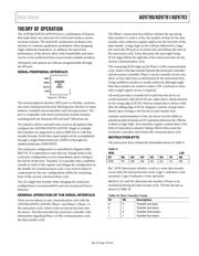
AD9780/AD9781/AD9783 Data Sheet
Rev. B | Page 24 of 32
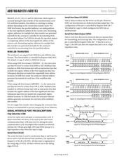
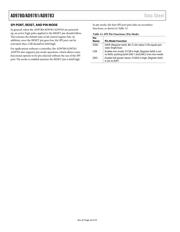
SPI PORT, RESET, AND PIN MODE
In general, when the AD9780/AD9781/AD9783 are powered
up, an active high pulse applied to the RESET pin should follow.
This ensures the default state of all control register bits. In
addition, once the RESET pin goes low, the SPI port can be
activated; thus, CSB should be held high.
For applications without a controller, the AD9780/AD9781/
AD9783 also supports pin mode operation, which allows some
functional options to be pin selected without the use of the SPI
port. Pin mode is enabled anytime the RESET pin is held high.
In pin mode, the four SPI port pins take on secondary
functions, as shown in Table 13.
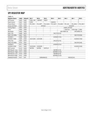
Table 13. SPI Pin Functions (Pin Mode)
Pin
Name Pin Mode Function
SDIO DATA (Register 0x02, Bit 7), bit value (1/0) equals pin
state (high/low).
CSB Enable mix mode. If CSB is high, Register 0x0A is set
to 0x05, putting both DAC1 and DAC2 into mix mode.
SDO Enable full power-down. If SDO is high, Register 0x03
is set to 0xFF.
器件 Datasheet 文档搜索
AiEMA 数据库涵盖高达 72,405,303 个元件的数据手册,每天更新 5,000 多个 PDF 文件
