Datasheet 搜索 > DA转换器 > ADI(亚德诺) > AD9780BCPZ 数据手册 > AD9780BCPZ 数据手册 9/32 页
 器件3D模型
¥ 218.897
AD9780BCPZ 数据手册 - ADI(亚德诺)
制造商:
ADI(亚德诺)
分类:
DA转换器
封装:
LFCSP-72
描述:
ANALOG DEVICES AD9780BCPZ 数模转换器, 双路, 12 bit, 并行、串行, 3.13V 至 3.47V, LFCSP, 72 引脚
Pictures:
3D模型
符号图
焊盘图
引脚图
产品图
页面导航:
引脚图在P7P8P9P20P24P31Hot
典型应用电路图在P29
原理图在P1P25
封装尺寸在P31
型号编码规则在P31
功能描述在P1P7P8P9P31
技术参数、封装参数在P1P3P4P5P6
应用领域在P1
电气规格在P10
导航目录
AD9780BCPZ数据手册
Page:
of 32 Go
若手册格式错乱,请下载阅览PDF原文件
Data Sheet AD9780/AD9781/AD9783
Rev. B | Page 9 of 32
06936-004
1
2
3
4
5
6
7
8
9
10
11
12
13
14
15
16
CVDD18
CVSS
CLKP
CLKN
CVSS
CVDD18
DVSS
DVDD18
D15P
D15N
D14P
D14N
D13P
D13N
D12P
D12N
17D11P
18D11N
19
20
21
22
23
24
25
26
27
28
29
30
31
32
33
34
D10P
D10N
D9P
D9N
D8P
D8N
DCOP
DCON
DVDD33
DVSS
DCIP
DCIN
D7P
D7N
D6P
D6N
35D5P
36D5N
54
53
52
51
50
49
48
47
46
45
44
43
42
41
40
39
38
37
FS ADJ
RESET
CSB
SCLK
SDIO
SDO
DVSS
DVDD18
D0N
D0P
D1N
D1P
D2N
D2P
D3N
D3P
D4N
D4P
72
71
70
69
68
67
66
65
64
63
62
61
60
59
58
57
56
55
AVDD33
AVDD33
AVSS
IOUT1P
IOUT1N
AVSS
AUX1P
AUX1N
AVSS
AUX2N
AUX2P
AVSS
IOUT2N
IOUT2P
AVSS
AVDD33
AVDD33
REFIO
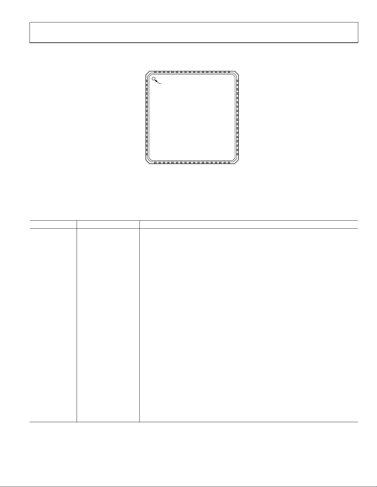
PIN 1
INDICATOR
AD9783
(TOP VIEW)
NOTES
1. EXPOSED PAD MUST BE
SOLDERED TO PCB AND
CONNECTED TO AVSS.
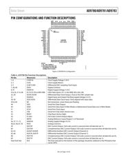
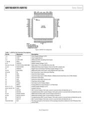
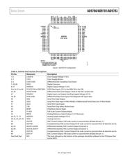
Figure 4. AD9783 Pin Configuration
Table 8. AD9783 Pin Function Descriptions
Pin No.
Mnemonic
Description
1, 6 CVDD18 Clock Supply Voltage (1.8 V).
2, 5 CVSS Clock Supply Return.
3, 4 CLKP, CLKN Differential DAC Sampling Clock Input.
7, 28, 48 DVSS Digital Common.
8, 47 DVDD18 Digital Supply Voltage (1.8 V).
9 to 24, 31 to 46 D15P, D15N to D0P, D0N LVDS Data Inputs. D15 is the MSB, D0 is the LSB.
25, 26 DCOP, DCON Differential Data Clock Output. Clock at the DAC sample rate.
27 DVDD33 Digital Input and Output Pad Ring Supply Voltage (3.3 V).
29, 30 DCIP, DCIN Differential Data Clock Input Clock aligned with input data.
49 SDO Serial Port Data Output.
50 SDIO Serial Port Data Input (4-Wire Mode) or Bidirectional Serial Data Line (3-Wire Mode).
51 SCLK Serial Port Clock Input.
52
CSB
Serial Port Chip Select (Active Low).
53 RESET Chip Reset (Active High).
54 FS ADJ Full-Scale Current Output Adjust.
55 REFIO Analog Reference Input/Output (1.2 V Nominal).
56, 57, 71, 72 AVDD33 Analog Supply Voltage (3.3 V).
58, 61, 64, 67, 70 AVSS Analog Common.
59 IOUT2P DAC Current Output. Full-scale current is sourced when all data bits are 1s.
60 IOUT2N Complementary DAC Current Output. Full-scale current is sourced when all data bits are 0s.
62, 63 AUX2P, AUX2N Differential Auxiliary DAC Current Output (Channel 2).
65, 66 AUX1N, AUX1P Differential Auxiliary DAC Current Output (Channel 1).
68 IOUT1N Complementary DAC Current Output. Full-scale current is sourced when all data bits are 0s.
69 IOUT1P DAC Current Output. Full-scale current is sourced when all data bits are 1s.
Heat Sink Pad N/A The heat sink pad on the bottom of the package should be soldered to the PCB plane that
carries AVSS.
器件 Datasheet 文档搜索
AiEMA 数据库涵盖高达 72,405,303 个元件的数据手册,每天更新 5,000 多个 PDF 文件
