Datasheet 搜索 > 放大器、缓冲器 > ADI(亚德诺) > ADA4922-1ACPZ-RL7 数据手册 > ADA4922-1ACPZ-RL7 数据手册 1/19 页
 器件3D模型
¥ 10.881
ADA4922-1ACPZ-RL7 数据手册 - ADI(亚德诺)
制造商:
ADI(亚德诺)
分类:
放大器、缓冲器
封装:
LFCSP-8
描述:
高压,差分18位ADC驱动器 High Voltage, Differential 18-Bit ADC Driver
Pictures:
3D模型
符号图
焊盘图
引脚图
产品图
页面导航:
导航目录
ADA4922-1ACPZ-RL7数据手册
Page:
of 19 Go
若手册格式错乱,请下载阅览PDF原文件
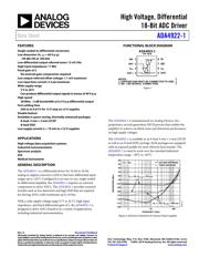
High Voltage, Differential
18-Bit ADC Driver
Data Sheet
ADA4922-1
Rev. A Document Feedback
Information furnished by Analog Devices is believed to be accurate and reliable. However, no
responsibility is assumed by Analog Devices for its use, nor for any infringements of patents or other
rights of third parties that may result from its use. Specifications subject to change without notice. No
license is granted by implication or otherwise under any patent or patent rights of Analog Devices.
Trademarks and registered trademarks are the property of their respective owners.
One Technology Way, P.O. Box 9106, Norwood, MA 02062-9106, U.S.A.
Tel: 781.329.4700 ©2005–2016 Analog Devices, Inc. All rights reserved.
Technical Support www.analog.com
FEATURES
Single-ended-to-differential conversion
Low distortion (V
O, dm
= 40 V p-p)
−99 dBc HD at 100 kHz
Low differential output referred noise: 12 nV/√Hz
High input impedance: 11 MΩ
Fixed gain of 2
No external gain components required
Low output-referred offset voltage: 1.1 mV maximum
Low input bias current: 3.5 μA maximum
Wide supply range
5 V to 26 V
Can produce differential output signals in excess of 40 V p-p
High speed
38 MHz, −3 dB bandwidth at 0.2 V p-p differential output
Fast settling time
200 ns to 0.01% for 12 V step on ±5 V supplies
Disable feature
Available in space-saving, thermally enhanced packages
8-lead, 3 mm × 3 mm LFCSP
8-lead SOIC
Low supply current: I
S
= 10 mA on ±12 V supplies
APPLICATIONS
High voltage data acquisition systems
Industrial instrumentation
Spectrum analysis
ATE
Medical instruments
GENERAL DESCRIPTION
The ADA4922-1 is a differential driver for 16-bit to 18-bit
analog-to-digital converters (ADCs) that have differential input
ranges up to ±20 V. Configured as an easy-to-use, single-ended-
to-differential amplifier, the ADA4922-1 requires no external
components to drive ADCs. The ADA4922-1 provides essential
benefits such as low distortion and high SNR that are required
for driving ADCs with resolutions up to 18 bits.
With a wide supply voltage range (5 V to 26 V), high input
impedance, and fixed differential gain of 2, the ADA4922-1 is
designed to drive ADCs found to in a variety of applications,
including industrial instrumentation.
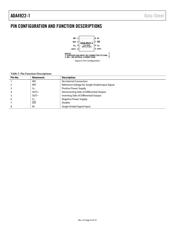
FUNCTIONAL BLOCK DIAGRAM
NIC
REF
V
S+
OUT+
DIS
IN
V
S–
OUT–
NOTES
1. EXPOSED PAD MUST BE CONNECTED TO GND.
2. NIC = NO INTERAL CONNECTION.
3
4
1
2
6
5
8
7
A
DA4922-1
TOP VIEW
05681-001
Figure 1.
The ADA4922-1 is manufactured on Analog Devices, Inc.,
proprietary, second-generation XFCB process that enables the
amplifier to achieve excellent noise and distortion performance
on high supply voltages.
The ADA4922-1 is available in an 8-lead 3 mm × 3 mm LFCSP
as well as an 8-lead SOIC package. Both packages are equipped
with an exposed paddle for more efficient heat transfer. The
ADA4922-1 is rated to work over the extended industrial
temperature range, −40°C to +85°C.
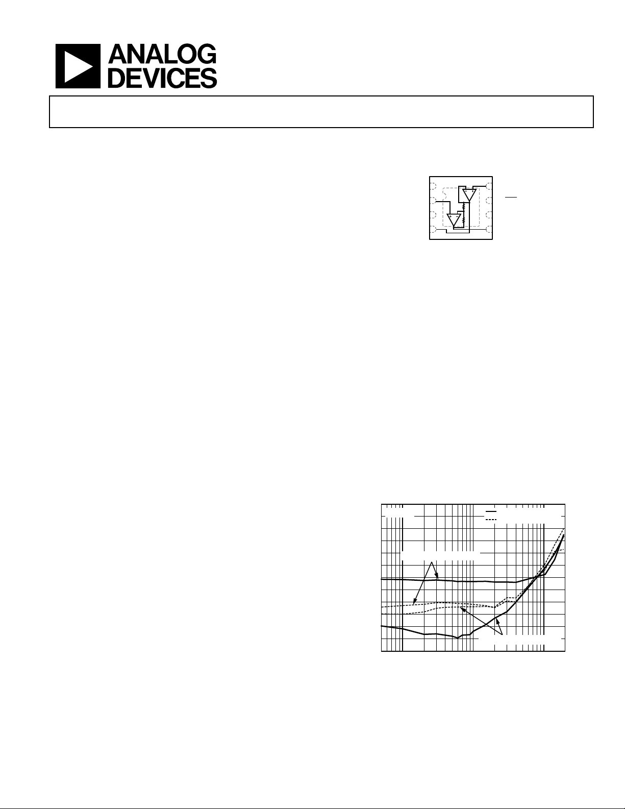
–84
–120
05681-012
FREQUENCY (kHz)
DISTORTION (dBc)
1 10 100
–87
–90
–93
–102
–99
–96
–105
–108
–111
–114
–117
SECOND HARMONIC
THIRD HARMONIC
R
L
= 2k
V
S
= 12V, V
O, dm
= 40V p-p
V
S
= 5V, V
O, dm
= 12V p-p
Figure 2. Harmonic Distortion for Various Power Supplies
器件 Datasheet 文档搜索
AiEMA 数据库涵盖高达 72,405,303 个元件的数据手册,每天更新 5,000 多个 PDF 文件
