Datasheet 搜索 > ADI(亚德诺) > ADA4937-1 数据手册 > ADA4937-1 数据手册 1/28 页


¥ 0
ADA4937-1 数据手册 - ADI(亚德诺)
制造商:
ADI(亚德诺)
描述:
超低失真,差分ADC驱动器 Ultralow Distortion, Differential ADC Driver
Pictures:
3D模型
符号图
焊盘图
引脚图
产品图
页面导航:
导航目录
ADA4937-1数据手册
Page:
of 28 Go
若手册格式错乱,请下载阅览PDF原文件
Ultralow Distortion
Differential ADC Driver
Data Sheet
ADA4937-1/ADA4937-2
Rev. F Document Feedback
Information furnished by Analog Devices is believed to be accurate and reliable. However, no
responsibility is assumed by Analog Devices for its use, nor for any infringements of patents or other
rights of third parties that may result from its use. Specifications subject to change without notice. No
license is granted by implication or otherwise under any patent or patent rights of Analog Devices.
Trademarks and registered trademarks are the property of their respective owners.
One Technology Way, P.O. Box 9106, Norwood, MA 02062-9106, U.S.A.
Tel: 781.329.4700 ©2007–2016 Analog Devices, Inc. All rights reserved.
Technical Support www.analog.com
FEATURES
Extremely low harmonic distortion (HD)
−112 dBc HD2 at 10 MHz
−84 dBc HD2 at 70 MHz
−77 dBc HD2 at 100 MHz
−102 dBc HD3 at 10 MHz
−91 dBc HD3 at 70 MHz
−84 dBc HD3 at 100 MHz
Low input voltage noise: 2.2 nV/√Hz
High speed
−3 dB bandwidth of 1.9 GHz, G = 1
Slew rate: 6000 V/μs, 25% to 75%
Fast overdrive recovery of 1 ns
0.5 mV typical offset voltage
Externally adjustable gain
Differential-to-differential or single-ended-to-differential
operation
Adjustable output common-mode voltage
Single-supply operation: 3.3 V to 5 V
APPLICATIONS
ADC drivers
Single-ended-to-differential converters
IF and baseband gain blocks
Differential buffers
Line drivers
GENERAL DESCRIPTION
The ADA4937-1/ADA4937-2 are low noise, ultralow distortion,
high speed differential amplifiers. They are an ideal choice for
driving high performance ADCs with resolutions up to 16 bits
from dc to 100 MHz. The adjustable level of the output common
mode allows the ADA4937-1/ADA4937-2 to match the input
of the ADC. The internal common-mode feedback loop also
provides exceptional output balance as well as suppression of
even-order harmonic distortion products.
With the ADA4937-1/ADA4937-2, differential gain configurations
are easily realized with a simple external feedback network of
four resistors that determine the closed-loop gain of the amplifier.
The ADA4937-1/ADA4937-2 are fabricated using Analog Devices,
Inc., proprietary silicon-germanium (SiGe), complementary
bipolar process, enabling them to achieve very low levels of
distortion with an input voltage noise of only 2.2 nV/√Hz.
The low dc offset and excellent dynamic performance of the
ADA4937-1/ADA4937-2 make them well-suited for a wide
variety of data acquisition and signal processing applications.
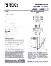
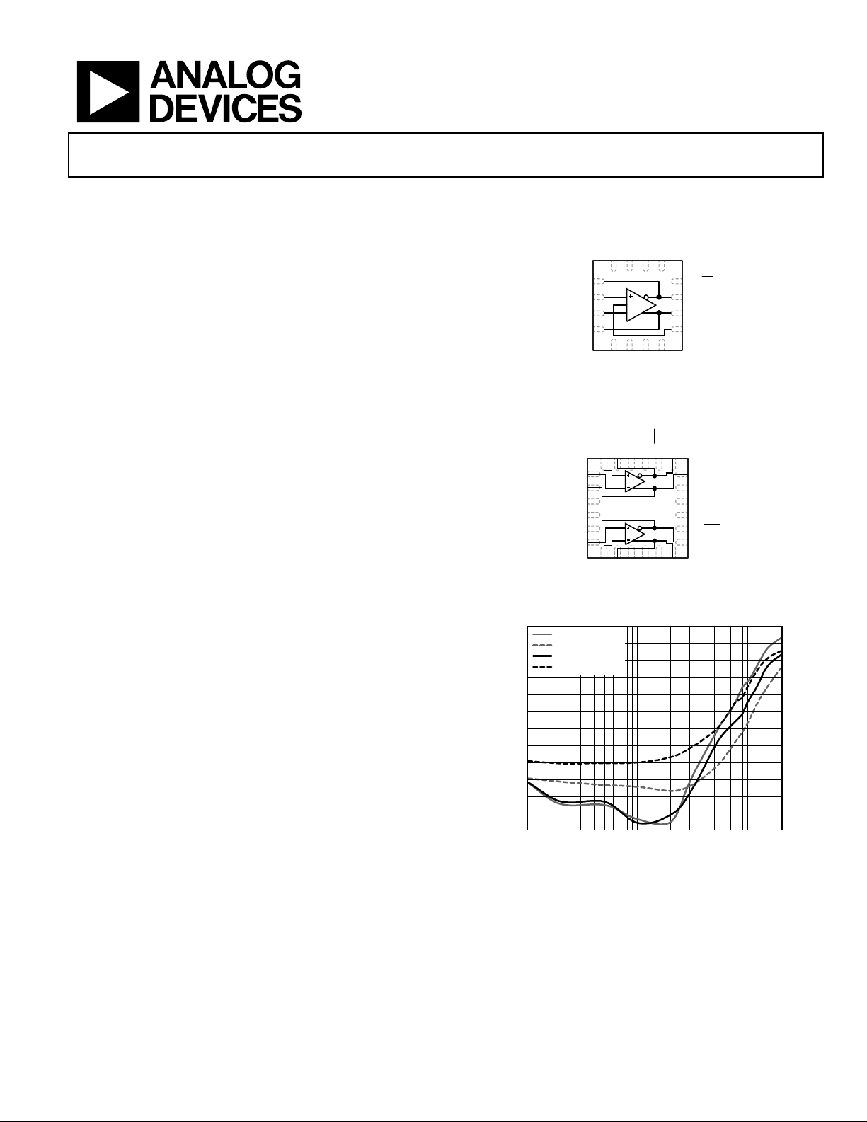
FUNCTIONAL BLOCK DIAGRAMS
06591-001
12
11
10
1
3
4
9
2
6
5
7
8
16
15
14
13
ADA4937-1
–
FB
+IN
–IN
+FB
PD
–V
S
–V
S
–V
S
–V
S
–OUT
+OUT
V
OCM
+V
S
+V
S
+V
S
+V
S
Figure 1. ADA4937-1
0
6591-002
2
1
3
4
5
6
18
17
16
15
14
13
+IN2
–FB2
+V
S1
+V
S1
+FB1
–IN1
–OUT2
PD2
–V
S2
–V
S2
V
OCM1
+OUT1
8
9
10
11
7
+FB2
+V
S2
+V
S2
V
OCM
2
12
+OUT2
–IN2
20
19
21
PD1
–OUT1
–V
S1
22
–V
S1
23
–FB1
24
+IN1
ADA4937-2
Figure 2. ADA4937-2
–
55
–60
–65
–70
–75
–80
–85
–90
–95
–100
–105
–110
–115
1 10 100
DISTORTION (dBc)
FREQUENCY (MHz)
HD2, V
S
=5.0V
HD3, V
S
=5.0V
HD2, V
S
=3.3V
HD3, V
S
=3.3V
06591-003
Figure 3. Harmonic Distortion vs. Frequency
The ADA4937-1/ADA4937-2 are available in a Pb-free, 3 mm ×
3 mm, 16-lead LFCSP (ADA4937-1, single) or a Pb-free, 4 mm ×
4 mm, 24-lead LFCSP (ADA4937-2, dual). The pinout has been
optimized to facilitate PCB layout and minimize distortion.
The ADA4937-1/ADA4937-2 are specified to operate over the
automotive (−40°C to +105°C) temperature range and between
3.3 V and 5 V supplies.
器件 Datasheet 文档搜索
AiEMA 数据库涵盖高达 72,405,303 个元件的数据手册,每天更新 5,000 多个 PDF 文件
