Datasheet 搜索 > AD转换器 > TI(德州仪器) > ADC0832CIWMX/NOPB 数据手册 > ADC0832CIWMX/NOPB 数据手册 15/42 页
 器件3D模型
¥ 0
ADC0832CIWMX/NOPB 数据手册 - TI(德州仪器)
制造商:
TI(德州仪器)
分类:
AD转换器
封装:
SOIC-14
Pictures:
3D模型
符号图
焊盘图
引脚图
产品图
页面导航:
典型应用电路图在P1
原理图在P4P6P12P15
封装尺寸在P30P31P32P33P39
焊盘布局在P40
标记信息在P30P31
封装信息在P30P31P32P33
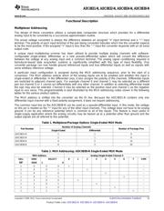
功能描述在P3P4P13P18
技术参数、封装参数在P1P3
应用领域在P19P42
电气规格在P4P5P7P8P16
导航目录
ADC0832CIWMX/NOPB数据手册
Page:
of 42 Go
若手册格式错乱,请下载阅览PDF原文件
ADC0831-N, ADC0832-N, ADC0834-N, ADC0838-N
www.ti.com
SNAS531B –AUGUST 1999–REVISED MARCH 2013
THE DIGITAL INTERFACE
A most important characteristic of these converters is their serial data link with the controlling processor. Using a
serial communication format offers two very significant system improvements; it allows more function to be
included in the converter package with no increase in package size and it can eliminate the transmission of low
level analog signals by locating the converter right at the analog sensor; transmitting highly noise immune digital
data back to the host processor.
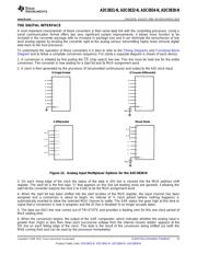
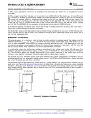
To understand the operation of these converters it is best to refer to the Timing Diagrams and Functional Block
Diagram and to follow a complete conversion sequence. For clarity a separate diagram is shown of each device.
1. A conversion is initiated by first pulling the CS (chip select) line low. This line must be held low for the entire
conversion. The converter is now waiting for a start bit and its MUX assignment word.
2. A clock is then generated by the processor (if not provided continuously) and output to the A/D clock input.
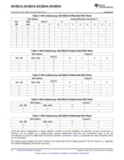
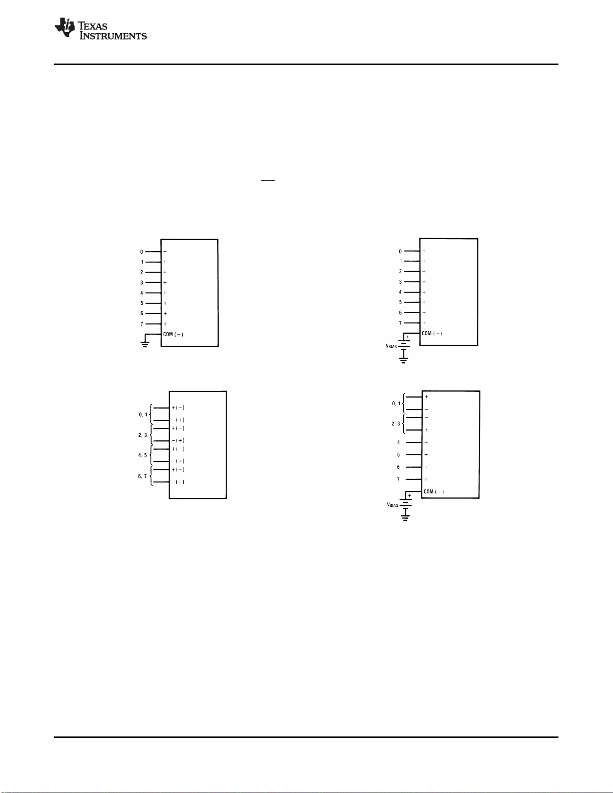
8 Single-Ended 8 Pseudo-Differential
4 Differential Mixed Mode
Figure 22. Analog Input Multiplexer Options for the ADC0838-N
3. On each rising edge of the clock the status of the data in (DI) line is clocked into the MUX address shift
register. The start bit is the first logic “1” that appears on this line (all leading zeros are ignored). Following the
start bit the converter expects the next 2 to 4 bits to be the MUX assignment word.
4. When the start bit has been shifted into the start location of the MUX register, the input channel has been
assigned and a conversion is about to begin. An interval of ½ clock period (where nothing happens) is
automatically inserted to allow the selected MUX channel to settle. The SAR status line goes high at this time to
signal that a conversion is now in progress and the DI line is disabled (it no longer accepts data).
5. The data out (DO) line now comes out of TRI-STATE and provides a leading zero for this one clock period of
MUX settling time.
6. When the conversion begins, the output of the SAR comparator, which indicates whether the analog input is
greater than (high) or less than (low) each successive voltage from the internal resistor ladder, appears at the
DO line on each falling edge of the clock. This data is the result of the conversion being shifted out (with the
MSB coming first) and can be read by the processor immediately.
Copyright © 1999–2013, Texas Instruments Incorporated Submit Documentation Feedback 15
Product Folder Links: ADC0831-N ADC0832-N ADC0834-N ADC0838-N
器件 Datasheet 文档搜索
AiEMA 数据库涵盖高达 72,405,303 个元件的数据手册,每天更新 5,000 多个 PDF 文件
