Datasheet 搜索 > AD转换器 > TI(德州仪器) > ADC0834CCWMX/NOPB 数据手册 > ADC0834CCWMX/NOPB 数据手册 3/39 页

¥ 46.135
ADC0834CCWMX/NOPB 数据手册 - TI(德州仪器)
制造商:
TI(德州仪器)
分类:
AD转换器
封装:
SOIC-14
描述:
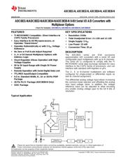
8位串行I / OA / D转换器与多路复用器选项 8-Bit Serial I/O A/D Converters with Multiplexer Options
Pictures:
3D模型
符号图
焊盘图
引脚图
产品图
页面导航:
典型应用电路图在P1
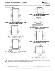
原理图在P4P6P12P15
封装尺寸在P30P31P32P33
标记信息在P30P31
封装信息在P30P31P32P33
功能描述在P3P4P13P18
技术参数、封装参数在P1P3
应用领域在P19P39
电气规格在P4P5P7P8P16

导航目录
ADC0834CCWMX/NOPB数据手册
Page:
of 39 Go
若手册格式错乱,请下载阅览PDF原文件
ADC0831-N, ADC0832-N, ADC0834-N, ADC0838-N
www.ti.com
SNAS531B –AUGUST 1999–REVISED MARCH 2013
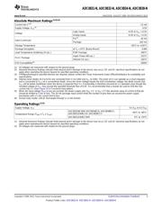
Absolute Maximum Ratings
(1)(2)(3)
Current into V
+(4)
15 mA
Supply Voltage, V
CC
(4)
6.5V
Logic Inputs −0.3V to V
CC
+ 0.3V
Voltage
Analog Inputs −0.3V to V
CC
+ 0.3V
Pin
(5)
±5 mA
Input Current per
Package ±20 mA
Storage Temperature −65°C to +150°C
Package Dissipation at T
A
= 25°C (Board Mount) 0.8W
Lead Temperature (Soldering 10 sec.) PDIP Package 260°C
Vapor Phase (60 sec.) 215°C
PLCC Package
Infrared (15 sec.) 220°C
ESD Susceptibility
(6)
2000V
(1) All voltages are measured with respect to the ground plugs.
(2) Absolute Maximum Ratings indicate limits beyond which damage to the device may occur. DC and AC electrical specifications do not
apply when operating the device beyond its specified operating conditions.
(3) If Military/Aerospace specified devices are required, please contact the Texas Instruments Sales Office/Distributors for availability and
specifications.
(4) Internal zener diodes (6.3 to 8.5V) are connected from V+ to GND and V
CC
to GND. The zener at V+ can operate as a shunt regulator
and is connected to V
CC
via a conventional diode. Since the zener voltage equals the A/D's breakdown voltage, the diode insures that
V
CC
will be below breakdown when the device is powered from V+. Functionality is therefore ensured for V+ operation even though the
resultant voltage at V
CC
may exceed the specified Absolute Max of 6.5V. It is recommended that a resistor be used to limit the max
current into V+. (See Figure 24 in Functional Description)
(5) When the input voltage (V
IN
) at any pin exceeds the power supply rails (V
IN
< V
−
or V
IN
> V
+
) the absolute value of current at that pin
should be limited to 5 mA or less. The 20 mA package input current limits the number of pins that can exceed the power supply
boundaries with a 5 mA current limit to four.
(6) Human body model, 100 pF discharged through a 1.5 kΩ resistor.
Operating Ratings
(1)(2)
Supply Voltage, V
CC
4.5 V
DC
to 6.3 V
DC
ADC0832/8CIWM ADC0834BCN, ADC0838BCV,
−40°C to +85°C
ADC0831/2/4/8CCN, ADC0838CCV
Temperature Range (T
MIN
≤ T
A
≤ T
MAX
)
ADC0831/2/4/8CCWM 0°C to +70°C
(1) Absolute Maximum Ratings indicate limits beyond which damage to the device may occur. DC and AC electrical specifications do not
apply when operating the device beyond its specified operating conditions.
(2) All voltages are measured with respect to the ground plugs.
Copyright © 1999–2013, Texas Instruments Incorporated Submit Documentation Feedback 3
Product Folder Links: ADC0831-N ADC0832-N ADC0834-N ADC0838-N
器件 Datasheet 文档搜索
AiEMA 数据库涵盖高达 72,405,303 个元件的数据手册,每天更新 5,000 多个 PDF 文件
