Datasheet 搜索 > National Semiconductor(美国国家半导体) > ADC122S021CIMM/NOPB 数据手册 > ADC122S021CIMM/NOPB 数据手册 5/20 页
 器件3D模型
¥ 14.752
ADC122S021CIMM/NOPB 数据手册 - National Semiconductor(美国国家半导体)
制造商:
National Semiconductor(美国国家半导体)
封装:
MSOP-8
Pictures:
3D模型
符号图
焊盘图
引脚图
产品图
页面导航:
引脚图在P2Hot
典型应用电路图在P17
原理图在P2
封装尺寸在P19
型号编码规则在P1
焊接温度在P3
功能描述在P1
技术参数、封装参数在P1P3P5P16
应用领域在P1P15
电气规格在P3P4P5P8
导航目录
ADC122S021CIMM/NOPB数据手册
Page:
of 20 Go
若手册格式错乱,请下载阅览PDF原文件
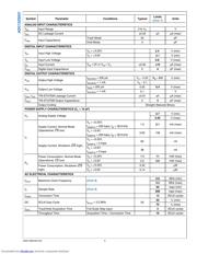
ADC122S021 Timing Specifications
The following specifications apply for V
A
= +2.7V to 5.25V, GND = 0V, f
SCLK
= 0.8 MHz to 3.2 MHz, f
SAMPLE
= 50 ksps to 200 ksps,
C
L
= 35 pF, Boldface limits apply for T
A
= T
MIN
to T
MAX
: all other limits T
A
= 25°C.
Symbol Parameter Conditions Typical
Limits
(Note 7)
Units
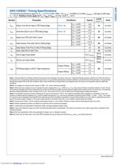
t
CSU
Setup Time SCLK High to CS Falling Edge (Note 10)
V
A
= +3.0V
−3.5
10 ns (min)
V
A
= +5.0V
−0.5
t
CLH
Hold time SCLK Low to CS Falling Edge (Note 10)
V
A
= +3.0V
+4.5
10 ns (min)
V
A
= +5.0V
+1.5
t
EN
Delay from CS Until DOUT active
V
A
= +3.0V
+4
30 ns (max)
V
A
= +5.0V
+2
t
ACC
Data Access Time after SCLK Falling Edge
V
A
= +3.0V
+14.5
30 ns (max)
V
A
= +5.0V
+13
t
SU
Data Setup Time Prior to SCLK Rising Edge +3 10 ns (min)
t
H
Data Valid SCLK Hold Time +3 10 ns (min)
t
CH
SCLK High Pulse Width
0.5 x t
SCLK
0.3 x
t
SCLK
ns (min)
t
CL
SCLK Low Pulse Width
0.5 x t
SCLK
0.3 x
t
SCLK
ns (min)
t
DIS
CS Rising Edge to DOUT High-Impedance
Output Falling
V
A
= +3.0V
1.8
20 ns (max)
V
A
= +5.0V
1.3
Output Rising
V
A
= +3.0V
1.0
V
A
= +5.0V
1.0
Note 1: Absolute Maximum Ratings indicate limits beyond which damage to the device may occur. Operating Ratings indicate conditions for which the device is
functional, but do not guarantee specific performance limits. For guaranteed specifications and test conditions, see the Electrical Characteristics. The guaranteed
specifications apply only for the test conditions listed. Some performance characteristics may degrade when the device is not operated under the listed test
conditions.
Note 2: All voltages are measured with respect to GND = 0V, unless otherwise specified.
Note 3: When the input voltage at any pin exceeds the power supply (that is, V
IN
< GND or V
IN
> V
A
), the current at that pin should be limited to 10 mA. The 20
mA maximum package input current rating limits the number of pins that can safely exceed the power supplies with an input current of 10 mA to two. The Absolute
Maximum Rating specification does not apply to the V
A
pin. The current into the V
A
pin is limited by the Analog Supply Voltage specification.
Note 4: The absolute maximum junction temperature (T
J
max) for this device is 150°C. The maximum allowable power dissipation is dictated by T
J
max, the
junction-to-ambient thermal resistance (θ
JA
), and the ambient temperature (T
A
), and can be calculated using the formula P
D
MAX = (T
J
max − T
A
)/θ
JA
. The values
for maximum power dissipation listed above will be reached only when the device is operated in a severe fault condition (e.g. when input or output pins are driven
beyond the power supply voltages, or the power supply polarity is reversed). Obviously, such conditions should always be avoided.
Note 5: Human body model is 100 pF capacitor discharged through a 1.5 kΩ resistor. Machine model is 220 pF discharged through zero ohms.
Note 6: Reflow temperature profiles are different for lead-free and non-lead-free packages.
Note 7: Tested limits are guaranteed to National's AOQL (Average Outgoing Quality Level).
Note 8: This is the frequency range over which the electrical performance is guaranteed. The device is functional over a wider range which is specified under
Operating Ratings.
Note 9: Min/max specification limits are guaranteed by design, test, or statistical analysis.
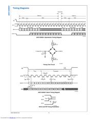
Note 10: Clock may be either high or low when CS is asserted as long as setup and hold times t
CSU
and t
CLH
are strictly observed.
.
5 www.national.com
ADC122S021
Downloaded from Elcodis.com electronic components distributor
器件 Datasheet 文档搜索
AiEMA 数据库涵盖高达 72,405,303 个元件的数据手册,每天更新 5,000 多个 PDF 文件
