Datasheet 搜索 > National Semiconductor(美国国家半导体) > ADC124S101CIMM 数据手册 > ADC124S101CIMM 数据手册 1/27 页
 器件3D模型
¥ 26.004
ADC124S101CIMM 数据手册 - National Semiconductor(美国国家半导体)
制造商:
National Semiconductor(美国国家半导体)
封装:
TFSOP-10
Pictures:
3D模型
符号图
焊盘图
引脚图
产品图
页面导航:
引脚图在P2Hot
典型应用电路图在P18
原理图在P2
封装尺寸在P22P24P25
标记信息在P22
封装信息在P22P23P24P25
焊接温度在P3
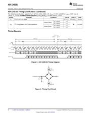
技术参数、封装参数在P1P3P5P6P17
应用领域在P1P16P27
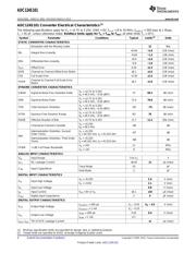
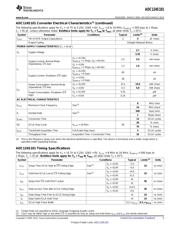
电气规格在P3P4P5P9P10P11P12P13P14P15P19
导航目录
ADC124S101CIMM数据手册
Page:
of 27 Go
若手册格式错乱,请下载阅览PDF原文件
1
2
3
4
5
6
7
8
9
10
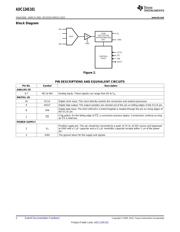
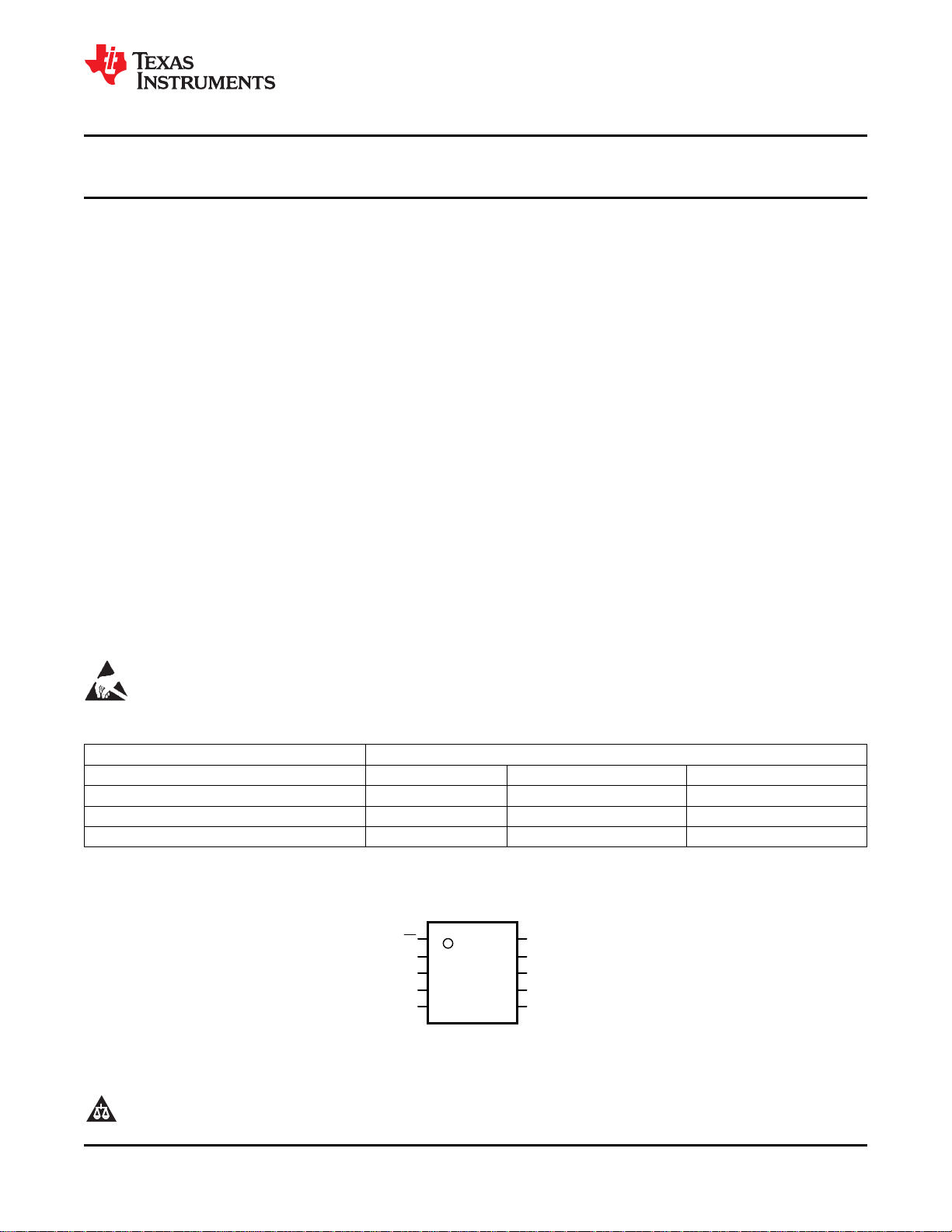
CS SCLK
DOUT
DIN
IN1
GND
IN4
IN3 IN2
V
A
ADC124S101
ADC124S101
www.ti.com
SNAS283D –MARCH 2005–REVISED MARCH 2013
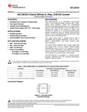
ADC124S101 4 Channel, 500 ksps to 1 Msps, 12-Bit A/D Converter
Check for Samples: ADC124S101
1
FEATURES
DESCRIPTION
The ADC124S101 is a low-power, four-channel
2
• Specified Over a Range of Sample Rates
CMOS 12-bit analog-to-digital converter with a high-
• Four Input Channels
speed serial interface. Unlike the conventional
• Variable Power Management
practice of specifying performance at a single sample
rate only, the ADC124S101 is fully specified over a
• Single Power Supply with 2.7V - 5.25V range
sample rate range of 500 ksps to 1 Msps. The
converter is based on a successive-approximation
APPLICATIONS
register architecture with an internal track-and-hold
• Portable Systems
circuit. It can be configured to accept up to four input
signals at inputs IN1 through IN4.
• Remote Data Acquisition
• Instrumentation and Control Systems
The output serial data is straight binary, and is
compatible with several standards, such as SPI™,
QSPI™, MICROWIRE, and many common DSP
KEY SPECIFICATIONS
serial interfaces.
• DNL: +0.9/−0.6 LSB (typ)
The ADC124S101 operates with a single supply that
• INL: ± 0.64 LSB (typ)
can range from +2.7V to +5.25V. Normal power
• SNR: 72.4 dB (typ)
consumption using a +3V or +5V supply is 4.3 mW
• Power Consumption
and 13.1 mW, respectively. The power-down feature
reduces the power consumption to just 0.14 µW using
– 3V Supply: 4.3 mW (typ)
a +3V supply, or 0.32 µW using a +5V supply.
– 5V Supply: 13.1 mW (typ)
The ADC124S101 is available in a 10-lead VSSOP
package. Operation over the industrial temperature
range of −40°C to +85°C.
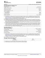
These devices have limited built-in ESD protection. The leads should be shorted together or the device placed in conductive foam
during storage or handling to prevent electrostatic damage to the MOS gates.
Table 1. PIN-COMPATIBLE ALTERNATIVES BY RESOLUTION AND SPEED
(1)
Resolution Specified for Sample Rate Range of:
50 to 200 ksps 200 to 500 ksps 500 ksps to 1 Msps
12-bit ADC124S021 ADC124S051 ADC124S101
10-bit ADC104S021 ADC104S051 ADC104S101
8-bit ADC084S021 ADC084S051 ADC084S101
(1) All devices are fully pin and function compatible.
Connection Diagram
Figure 1. 10-Lead VSSOP
See DGS Package
1
Please be aware that an important notice concerning availability, standard warranty, and use in critical applications of
Texas Instruments semiconductor products and disclaimers thereto appears at the end of this data sheet.
2All trademarks are the property of their respective owners.
PRODUCTION DATA information is current as of publication date.
Copyright © 2005–2013, Texas Instruments Incorporated
Products conform to specifications per the terms of the Texas
Instruments standard warranty. Production processing does not
necessarily include testing of all parameters.
器件 Datasheet 文档搜索
AiEMA 数据库涵盖高达 72,405,303 个元件的数据手册,每天更新 5,000 多个 PDF 文件
