Datasheet 搜索 > 时钟缓冲器、驱动器、锁相环 > ADI(亚德诺) > ADCLK905BCPZ-R2 数据手册 > ADCLK905BCPZ-R2 数据手册 7/16 页
 器件3D模型
¥ 0.145
ADCLK905BCPZ-R2 数据手册 - ADI(亚德诺)
制造商:
ADI(亚德诺)
分类:
时钟缓冲器、驱动器、锁相环
封装:
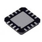
LFCSP-16
描述:
时钟缓冲器 Ultrafast SiGe ECL
Pictures:
3D模型
符号图
焊盘图
引脚图
产品图
页面导航:
引脚图在P6P7Hot
典型应用电路图在P1P12
原理图在P11P13
封装尺寸在P14
型号编码规则在P14
功能描述在P1P6P7
技术参数、封装参数在P1P3P5
应用领域在P1P11
电气规格在P3P8
导航目录
ADCLK905BCPZ-R2数据手册
Page:
of 16 Go
若手册格式错乱,请下载阅览PDF原文件
ADCLK905/ADCLK907/ADCLK925
Rev. 0 | Page 7 of 16
Pin No. Mnemonic Description
10 Q2 Noninverting Output 2.
11
Q1
Inverting Output 1.
12 Q1 Noninverting Output 1.
15 V
REF
1 Reference Voltage 1. Reference voltage for biasing ac-coupled inputs, Channel 1.
16 V
T
1 Center Tap 1. Center tap of 100 Ω input resistor, Channel 1.
Heat Sink NC
No Connect. The metallic back surface of the package is not electrically connected to any part of the circuit.
It can be left floating for optimal electrical isolation between the package handle and the substrate of the die.
It can also be soldered to the application board if improved thermal and/or mechanical stability is desired.
Exposed metal at the corners of the package is connected to this back surface. Allow sufficient clearance
to vias and other components.
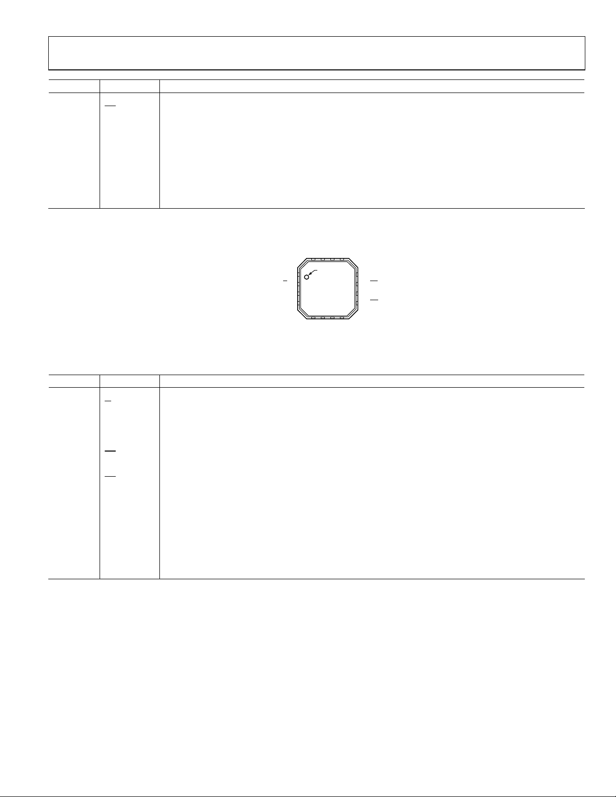
PIN 1
INDICATOR
NC = NO CONNECT
1D
2D
3NC
4NC
11 Q1
12 Q1
10 Q2
9Q2
5
NC
6
NC
7
V
EE
8
V
CC
15
V
REF
16
V
T
14
V
EE
13
V
CC
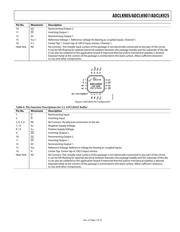
ADCLK925
TOP VIEW
(Not to Scale)
06318-006
Figure 6. ADCLK925 Pin Configuration
Table 6. Pin Function Descriptions for 1:2 ADCLK925 Buffer
Pin No. Mnemonic Description
1 D Noninverting Input.
2
D
Inverting Input.
3, 4, 5, 6 NC No Connect. No physical connection to the die.
7, 14 V
EE
Negative Supply Voltage.
8, 13 V
CC
Positive Supply Voltage.
9
Q2
Inverting Output 2.
10 Q2 Noninverting Output 2.
11
Q1
Inverting Output 1.
12 Q1 Noninverting Output 1.
15 V
REF
Reference Voltage. Reference voltage for biasing ac-coupled inputs.
16 V
T
Center Tap. Center tap of 100 Ω input resistor.
Heat Sink NC
No Connect. The metallic back surface of the package is not electrically connected to any part of the circuit.
It can be left floating for optimal electrical isolation between the package handle and the substrate of the die.
It can also be soldered to the application board if improved thermal and/or mechanical stability is desired.
Exposed metal at the corners of the package is connected to this back surface. Allow sufficient clearance
to vias and other components.
器件 Datasheet 文档搜索
AiEMA 数据库涵盖高达 72,405,303 个元件的数据手册,每天更新 5,000 多个 PDF 文件
