Datasheet 搜索 > ADI(亚德诺) > ADCMP573BCP 数据手册 > ADCMP573BCP 数据手册 6/14 页


¥ 0
ADCMP573BCP 数据手册 - ADI(亚德诺)
制造商:
ADI(亚德诺)
封装:
HVQCCN
描述:
超快3.3 V单电源比较器 Ultrafast 3.3 V Single-Supply Comparators
Pictures:
3D模型
符号图
焊盘图
引脚图
产品图
页面导航:
导航目录
ADCMP573BCP数据手册
Page:
of 14 Go
若手册格式错乱,请下载阅览PDF原文件
ADCMP572/ADCMP573 Data Sheet
Rev. B | Page 6 of 14
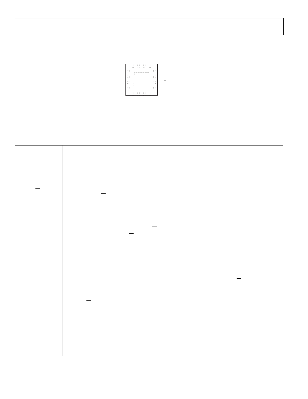
PIN CONFIGURATION AND FUNCTION DESCRIPTIONS
04409-026
LE
Q
12
11
10
1
3
4
9
2
6
5
7
8
16
15
14
13
NOTES
1. LEAVE EPAD FLOATING UNLESS IMPROVED THERMAL OR MECHANICAL
STABILITY IS DESIRED, IN WHICH CASE SOLDER IT TO THE APPLICATION BOARD.
V
TP
V
P
V
N
V
TN
V
CCO
GND
HYS
GND
V
CCI
Q
V
CCO
V
CCI
LE
V
CCO
/V
TT
ADCMP572
ADCMP573
TOP VIEW
Figure 2. ADCMP572/ADCMP573 Pin Configuration
Table 3. Pin Function Descriptions
Pin
No. Mnemonic Description
1 V
TP
Termination Resistor Return Pin for V
P
Input.
2 V
P
Noninverting Analog Input.
3 V
N
Inverting Analog Input.
4 V
TN
Termination Resistor Return Pin for V
N
Input.
5, 16 V
CCI
Positive Supply Voltage for Input Stage.
6
LE
Latch Enable Input Pin, Inverting Side.
In compare mode (LE
= low), the output tracks changes at the input of the comparator.
In latch mode (LE
= high), the output reflects the input state just prior to the comparator’s being placed into latch
mode. LE
must be driven in complement with LE.
7 LE
Latch Enable Input Pin, Noninverting Side.
In compare mode (LE = high), the output tracks changes at the input of the comparator.
In latch mode (LE = low), the output reflects the input state just prior to the comparator’s being placed into latch
mode. LE must be driven in complement with LE
.
8 V
CCO
/V
TT
Termination Return Pin for the LE/LE
Input Pins.
For the ADCMP572 (CML output stage), this pin is internally connected to and also should be externally connected
to the positive V
CCO
supply.
For the ADCMP573 (RSPECL output stage), this pin should normally be connected to the V
CCO
– 2 V termination
potential.
9, 12 V
CCO
Positive Supply Voltage for the CML/RSPECL Output Stage.
13, 15 GND Ground.
10
Q
Inverting Output. Q is at logic low if the analog voltage at the noninverting input, V
P
, is greater than the analog
voltage at the inverting input, V
N
, provided the comparator is in compare mode. See the LE/LE descriptions (Pins 6
and 7) for more information.
11 Q
Noninverting Output. Q is at logic high if the analog voltage at the noninverting input V
P
is greater than the analog
voltage at the inverting input, V
N
, provided the comparator is in compare mode.
See the LE/LE
descriptions (Pins 6 and 7) for more information.
14 HYS
Hysteresis Control Pin. Leave this pin disconnected for zero hysteresis. Connect to GND with a suitably sized
resistor to add the desired amount of hysteresis. Refer to Figure 7 for proper sizing of R
HYS
hysteresis control
resistor.
Isolated
Heat Sink
The metallic back surface of the package is not electrically connected to any part of the circuit, and it can be left
floating for best electrical isolation between the package handle and the substrate of the die. However, it can be
soldered to the application board if improved thermal and/or mechanical stability is desired. Exposed metal at
package corners is connected to the heat sink paddle.
EPAD
Exposed Pad. Leave EPAD floating unless improved thermal or mechanical stability is desired, in which case solder
it to the application board.
器件 Datasheet 文档搜索
AiEMA 数据库涵盖高达 72,405,303 个元件的数据手册,每天更新 5,000 多个 PDF 文件
