Datasheet 搜索 > 接口芯片 > ADI(亚德诺) > ADG1401BRMZ-REEL7 数据手册 > ADG1401BRMZ-REEL7 数据手册 1/16 页
 器件3D模型
¥ 22.05
ADG1401BRMZ-REEL7 数据手册 - ADI(亚德诺)
制造商:
ADI(亚德诺)
分类:
接口芯片
封装:
MSOP-8
描述:
1 Ω导通电阻, ±15 V / + 12 V / ± 5 V的iCMOS单刀单掷开关 1 Ω On Resistance, ±15 V/+12 V/±5 V iCMOS SPST Switches
Pictures:
3D模型
符号图
焊盘图
引脚图
产品图
页面导航:

导航目录
ADG1401BRMZ-REEL7数据手册
Page:
of 16 Go
若手册格式错乱,请下载阅览PDF原文件
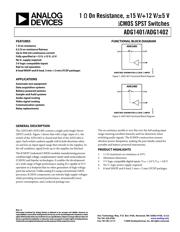
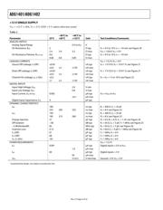
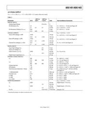
1 Ω On Resistance, ±15 V/+12 V/±5 V
iCMOS SPST Switches
ADG1401/ADG1402
Rev. 0
Information furnished by Analog Devices is believed to be accurate and reliable. However, no
responsibility is assumed by Analog Devices for its use, nor for any infringements of patents or other
rights of third parties that may result from its use. Specifications subject to change without notice. No
license is granted by implication or otherwise under any patent or patent rights of Analog Devices.
Trademarks and registered trademarks are the property of their respective owners.
One Technology Way, P.O. Box 9106, Norwood, MA 02062-9106, U.S.A.
Tel: 781.329.4700 www.analog.com
Fax: 781.461.3113 ©2009 Analog Devices, Inc. All rights reserved.
FEATURES
1 Ω on resistance
0.2 Ω on resistance flatness
Up to 430 mA continuous current
Fully specified at +12 V, ±15 V, ±5 V
No V
L
supply required
3 V logic-compatible inputs
Rail-to-rail operation
8-lead MSOP and 8-lead, 3 mm × 2 mm LFCSP packages
APPLICATIONS
Automatic test equipment
Data acquisition systems
Battery-powered systems
Sample-and-hold systems
Audio signal routing
Video signal routing
Communication systems
Relay replacements
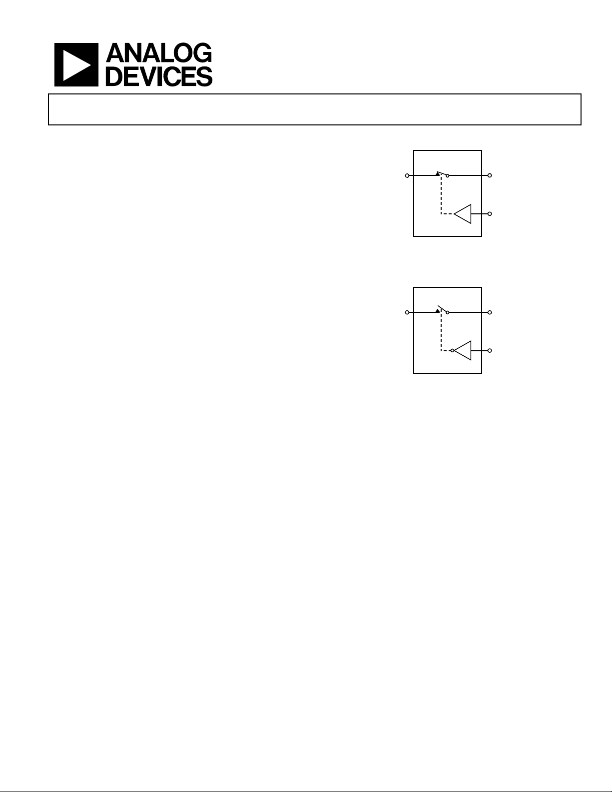
FUNCTIONAL BLOCK DIAGRAM
D
IN
S
ADG1401
SWITCHES SHOWN FOR A LOGIC 1 INPUT
08486-001
Figure 1. ADG1401 Functional Block Diagram
D
IN
S
ADG1402
SWITCHES SHOWN FOR A LOGIC 1 INPUT
08486-002
Figure 2. ADG1402 Functional Block Diagram
GENERAL DESCRIPTION
The ADG1401/ADG1402 contain a single-pole/single-throw
(SPST) switch. Figure 1 shows that with a logic input of 1, the
switch of the ADG1401 is closed and that of the ADG1402 is
open. Each switch conducts equally well in both directions when
on and has an input signal range that extends to the supplies. In
the off condition, signal levels up to the supplies are blocked.
The iCMOS® (industrial CMOS) modular manufacturing process
combines high voltage, complementary metal-oxide semiconductor
(CMOS) and bipolar technologies. It enables the development
of a wide range of high performance analog ICs capable of 33 V
operation in a footprint that no other generation of high voltage
parts has achieved. Unlike analog ICs using conventional CMOS
processes, iCMOS components can tolerate high supply voltages
while providing increased performance, dramatically lower
power consumption, and a reduced package size.
The on resistance profile is very flat over the full analog input
range ensuring excellent linearity and low distortion when
switching audio signals. The iCMOS construction ensures
ultralow power dissipation, making the part ideally suited for
portable and battery-powered instruments.
PRODUCT HIGHLIGHTS
1. 1.3 Ω maximum on resistance at 25°C.
2. Minimum distortion.
3. 3 V logic-compatible digital inputs: V
INH
= 2.0 V, V
INL
= 0.8 V.
4. No V
L
logic power supply required.
5. 8-lead MSOP and 8-lead, 3 mm × 2 mm LFCSP packages.
器件 Datasheet 文档搜索
AiEMA 数据库涵盖高达 72,405,303 个元件的数据手册,每天更新 5,000 多个 PDF 文件
