Datasheet 搜索 > 接口芯片 > ADI(亚德诺) > ADG408BRZ-REEL 数据手册 > ADG408BRZ-REEL 数据手册 1/15 页
 器件3D模型
¥ 10.07
ADG408BRZ-REEL 数据手册 - ADI(亚德诺)
制造商:
ADI(亚德诺)
分类:
接口芯片
封装:
SOIC-16
描述:
LC2MOS,8通道,高性能模拟多路复用器
Pictures:
3D模型
符号图
焊盘图
引脚图
产品图
页面导航:
导航目录
ADG408BRZ-REEL数据手册
Page:
of 15 Go
若手册格式错乱,请下载阅览PDF原文件
LC
2
MOS 4-/8-Channel
High Performance Analog Multiplexers
Data Sheet
ADG408/ADG409
Rev. D Document Feedback
Information furnished by Analog Devices is believed to be accurate and reliable. However, no
responsibility is assumed by Analog Devices for its use, nor for any infringements of patents or other
rights of third parties that may result from its use. Specifications subject to change without notice. No
license is granted by implication or otherwise under any patent or patent rights of Analog Devices.
Trademarks and registered trademarks are the property of their respective owners.
One Technology Way, P.O. Box 9106, Norwood, MA 02062-9106, U.S.A.
Tel: 781.329.4700 ©2001–2015 Analog Devices, Inc. All rights reserved.
Technical Support www.analog.com
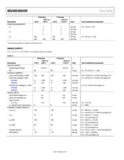
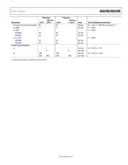
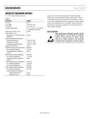
FEATURES
44 V supply maximum ratings
V
SS
to V
DD
analog signal range
Low on resistance (100 Ω maximum)
Low power (I
SUPPLY
< 75 μA)
Fast switching
Break-before-make switching action
Plug-in replacement for DG408/DG409
APPLICATIONS
Audio and video routing
Automatic test equipment
Data acquisition systems
Battery-powered systems
Sample-and-hold systems
Communication systems
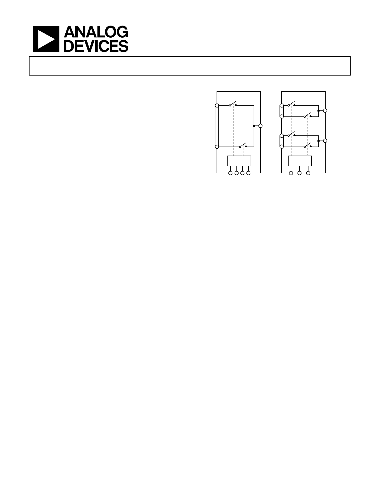
FUNCTIONAL BLOCK DIAGRAMS
ADG408
S1
S8
D
ADG409
S1A
S4B
DA
DB
S4A
S1B
1-OF-4
DECODER
1-OF-8
DECODER
A0 A1 ENA0 A1 A2 EN
00027-001
Figure 1.
GENERAL DESCRIPTION
The ADG408/ADG409 are monolithic CMOS analog multiplexers
comprising eight single channels and four differential channels,
respectively. The ADG408 switches one of eight inputs to a
common output as determined by the 3-bit binary address lines
A0, A1, and A2. The ADG409 switches one of four differential
inputs to a common differential output, as determined by the
2-bit binary address lines A0 and A1. An EN input on both devices
is used to enable or disable the device. When the device is disabled,
all channels are switched off.
The ADG408/ADG409 are designed on an enhanced LC
2
MOS
process that provides low power dissipation yet gives high
switching speed and low on resistance. Each channel conducts
equally well in both directions when on and has an input signal
range that extends to the supplies. In the off condition, signal levels
up to the supplies are blocked. All channels exhibit break-before-
make switching action, preventing momentary shorting when
switching channels. Inherent in the design is low charge injection
for minimum transients when switching the digital inputs.
The ADG408/ADG409 are improved replacements for the
DG408/DG409 analog multiplexers.
PRODUCT HIGHLIGHTS
1. Extended Signal Range. The ADG408/ADG409 are
fabricated on an enhanced LC
2
MOS process, giving an
in
creased signal range that extends to the supply rails.
2. Low Power Dissipation.
3. Low R
ON
.
4. S
ingle-Supply Operation. For applications where the
analog signal is unipolar, the ADG408/ADG409 can
be
operated from a single rail power supply. The parts are
fully specified with a single 12 V power supply and remain
functional with single supplies as low as 5 V.
器件 Datasheet 文档搜索
AiEMA 数据库涵盖高达 72,405,303 个元件的数据手册,每天更新 5,000 多个 PDF 文件
