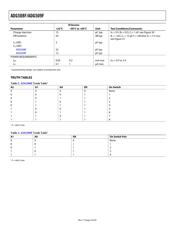
Datasheet 搜索 > 接口芯片 > ADI(亚德诺) > ADG509FBRN 数据手册 > ADG509FBRN 数据手册 1/20 页
 器件3D模型
¥ 7.264
ADG509FBRN 数据手册 - ADI(亚德诺)
制造商:
ADI(亚德诺)
分类:
接口芯片
封装:
SOIC-16
描述:
4/8通道故障保护模拟多路复用器 4/8 Channel Fault-Protected Analog Multiplexers
Pictures:
3D模型
符号图
焊盘图
引脚图
产品图
页面导航:
导航目录
ADG509FBRN数据手册
Page:
of 20 Go
若手册格式错乱,请下载阅览PDF原文件
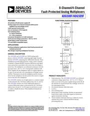
8-Channel/4-Channel
Fault-Protected Analog Multiplexers
ADG508F/ADG509F
Rev. F
Information furnished by Analog Devices is believed to be accurate and reliable. However, no
responsibility is assumed by Analog Devices for its use, nor for any infringements of patents or other
rights of third parties that may result from its use. Specifications subject to change without notice. No
license is granted by implication or otherwise under any patent or patent rights of Analog Devices.
Trademarks and registered trademarks are the property of their respective owners.
One Technology Way, P.O. Box 9106, Norwood, MA 02062-9106, U.S.A.
Tel: 781.329.4700 www.analog.com
Fax: 781.461.3113 ©2001–2011 Analog Devices, Inc. All rights reserved.
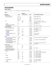
FEATURES
All switches off with power supply off
Analog output of on channel clamped within power
supplies if an overvoltage occurs
Latch-up proof construction
Low on resistance (270 Ω typical)
Fast switching times
t
ON
: 230 ns maximum
t
OFF
: 130 ns maximum
Low power dissipation (3.3 mW maximum)
Fault and overvoltage protection (−40 V to +55 V)
Break-before-make construction
TTL and CMOS compatible inputs
APPLICATIONS
Existing multiplexer applications (both fault-protected and
nonfault-protected)
New designs requiring multiplexer functions
GENERAL DESCRIPTION
The ADG508F and ADG509F are CMOS analog multi-
plexers, with the ADG508F comprising eight single channels
and the ADG509F comprising four differential channels. These
multiplexers provide fault protection. Using a series n-channel,
p-channel, n-channel MOSFET structure, both device and signal
source protection is provided in the event of an overvoltage or
power loss. The multiplexer can withstand continuous overvolt-
age inputs from −40 V to +55 V. During fault conditions with
power supplies off, the multiplexer input (or output) appears as
an open circuit and only a few nanoamperes of leakage current
will flow. This protects not only the multiplexer and the circuitry
driven by the multiplexer, but also protects the sensors or signal
sources that drive the multiplexer.
The ADG508F switches one of eight inputs to a common output
as determined by the 3-bit binary address lines A0, A1, and A2.
The ADG509F switches one of four differential inputs to a
common differential output as determined by the 2-bit binary
address lines A0 and A1. An EN input on each device is used
to enable or disable the device. When disabled, all channels are
switched off.
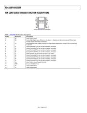
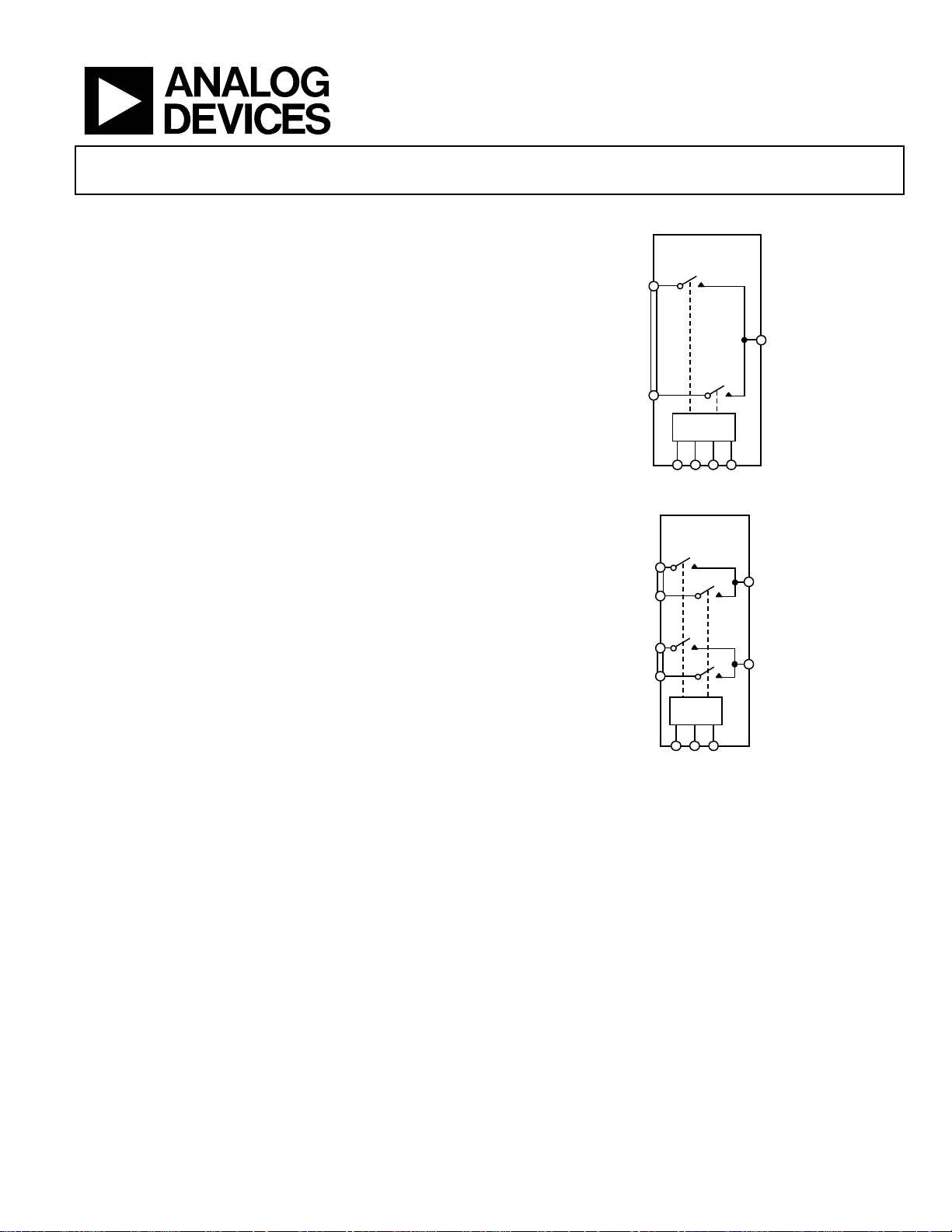
FUNCTIONAL BLOCK DIAGRAMS
S1
S8
A0
D
ADG508F
A1 A2 EN
1 OF 8
DECODER
00035-001
Figure 1.
S1A
A0
DA
ADG509F
A1
S4A
S1B
S4B
DB
EN
1 OF 4
DECODER
00035-101
Figure 2.
PRODUCT HIGHLIGHTS
1. Fault protection. The ADG508F/ADG509F can withstand
continuous voltage inputs from −40 V to +55 V. When a
fault occurs due to the power supplies being turned off, all
the channels are turned off and only a leakage current of a
few nanoamperes flows.
2. On channel saturates while fault exists.
3. Low R
ON
.
4. Fast switching times.
5. Break-before-make switching. Switches are guaranteed
break-before-make so that input signals are protected
against momentary shorting.
6. Trench isolation eliminates latch-up. A dielectric trench
separates the p and n-channel MOSFETs thereby
preventing latch-up.
器件 Datasheet 文档搜索
AiEMA 数据库涵盖高达 72,405,303 个元件的数据手册,每天更新 5,000 多个 PDF 文件
