Datasheet 搜索 > 电源配件 > ADI(亚德诺) > ADM1166ACPZ-REEL 数据手册 > ADM1166ACPZ-REEL 数据手册 1/33 页
 器件3D模型
¥ 146.495
ADM1166ACPZ-REEL 数据手册 - ADI(亚德诺)
制造商:
ADI(亚德诺)
分类:
电源配件
封装:
LFCSP-40
描述:
超序与余量控制和非易失故障记录 Super Sequencer with Margining Control and Nonvolatile Fault Recording
Pictures:
3D模型
符号图
焊盘图
引脚图
产品图
页面导航:
导航目录
ADM1166ACPZ-REEL数据手册
Page:
of 33 Go
若手册格式错乱,请下载阅览PDF原文件
Super Sequencer with Margining Control
and Nonvolatile Fault Recording
Data Sheet
ADM1166
Rev. A Document Feedback
Information furnished by Analog Devices is believed to be accurate and reliable. However, no
responsibility is assumed by Analog Devices for its use, nor for any infringements of patents or other
rights of third parties that may result from its use. Specifications subject to change without notice. No
license is granted by implication or otherwise under any patent or patent rights of Analog Devices.
Trademarks and registered trademarks are the property of their respective owners.
One Technology Way, P.O. Box 9106, Norwood, MA 02062-9106, U.S.A.
Tel: 781.329.4700 ©2010–2015 Analog Devices, Inc. All rights reserved.
Technical Support www.analog.com
FEATURES
Complete supervisory and sequencing solution for up to
10 supplies
16 event deep black box nonvolatile fault recording
10 supply fault detectors enable supervision of supplies to
<0.5% accuracy at all voltages at 25°C
<1.0% accuracy across all voltages and temperatures
5 selectable input attenuators allow supervision of supplies to
14.4 V on VH and 6 V on VP1 to VP4 (VPx)
5 dual-function inputs, VX1 to VX5 (VXx)
High impedance input to supply fault detector with
thresholds between 0.573 V and 1.375 V
General-purpose logic input
10 programmable driver outputs, PDO1 to PDO10 (PDOx)
Open-collector with external pull-up
Push/pull output, driven to VDDCAP or VPx
Open collector with weak pull-up to VDDCAP or VPx
Internally charge-pumped high drive for use with external
N-FET (PDO1 to PDO6 only)
SE implements state machine control of PDO outputs
State changes conditional on input events
Enables complex control of boards
Power-up and power-down sequence control
Fault event handling
Interrupt generation on warnings
Watchdog function can be integrated in SE
Program software control of sequencing through SMBus
Complete voltage-margining solution for 6 voltage rails
6 voltage output 8-bit DACs (0.300 V to 1.551 V) allow voltage
adjustment via dc-to-dc converter trim/feedback node
12-bit ADC for readback of all supervised voltages
2 auxiliary (single-ended) ADC inputs
Reference input (REFIN) has 2 input options
Driven directly from 2.048 V (±0.25%) REFOUT pin
More accurate external reference for improved ADC
performance
Device powered by the highest of VPx, VH for improved
redundancy
User EEPROM: 256 bytes
Industry-standard 2-wire bus interface (SMBus)
Guaranteed PDO low with VH, VPx = 1.2 V
Available in 40-lead, 6 mm × 6 mm LFCSP and
48-lead, 7 mm × 7 mm TQFP packages
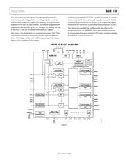
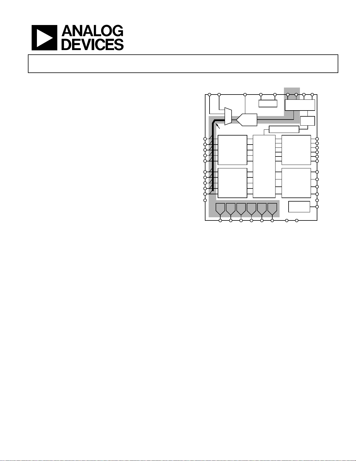
FUNCTIONAL BLOCK DIAGRAM
PDO7
PDO8
PDO9
PDO10
PDOGND
VDDCAP
VDD
ARBITRATOR
DAC1
V
OUT
DAC
DAC2
V
OUT
DAC
DAC3
V
OUT
DAC
DAC4
V
OUT
DAC
DAC5
V
OUT
DAC
DAC6
V
OUT
DAC
GND
VCCP
VX1
VX2
VX3
VX4
VX5
VP1
VP2
VP3
VP4
VH
A
GND
PROGRAMMABLE
RESET
GENERATORS
(SFDs)
DUAL-
FUNCTION
INPUTS
(LOGIC INPUTS
OR
SFDs)
SEQUENCING
ENGINE
CONFIGURABLE
OUTPUT
DRIVERS
(LV CAPABLE
OF DRIVING
LOGIC SIGNALS)
PDO1
PDO2
PDO3
PDO4
PDO5
PDO6
SDA SCL A1 A0
SMBus
INTERFACE
REFOUTREFINAUX2AUX1 REFGND
VREF
FAULT RECORDING
12-BIT
SAR ADC
MUX
EEPROM
CLOSED-LOOP
MARGINING SYSTEM
ADM1166
CONFIGURABLE
OUTPUT
DRIVERS
(HV CAPABLE OF
DRIVING GATES
OF N-FET)
09332-001
Figure 1.
APPLICATIONS
Central office systems
Servers/routers
Multivoltage system line cards
DSP/FPGA supply sequencing
In-circuit testing of margined supplies
GENERAL DESCRIPTION
The ADM1166 Super Sequencer® is a configurable supervisory/
sequencing device that offers a single-chip solution for supply
monitoring and sequencing in multiple-supply systems. In addition
to these functions, the ADM1166 integrates a 12-bit ADC and
six 8-bit voltage output DACs. These circuits can be used to
implement a closed-loop margining system that enables supply
adjustment by altering either the feedback node or reference of
a dc-to-dc converter using the DAC outputs.
Supply margining can be performed with a minimum of external
components. The margining loop can be used for in-circuit testing
of a board during production (for example, to verify board func-
tionality at −5% of nominal supplies), or it can be used dynamically
to accurately control the output voltage of a dc-to-dc converter.
For more information about the ADM1166 register map, refer
to the AN-698 Application Note.
器件 Datasheet 文档搜索
AiEMA 数据库涵盖高达 72,405,303 个元件的数据手册,每天更新 5,000 多个 PDF 文件
