Datasheet 搜索 > 接口芯片 > ADI(亚德诺) > ADM3070EARZ-REEL7 数据手册 > ADM3070EARZ-REEL7 数据手册 9/20 页

 器件3D模型
¥ 9.228
ADM3070EARZ-REEL7 数据手册 - ADI(亚德诺)
制造商:
ADI(亚德诺)
分类:
接口芯片
封装:
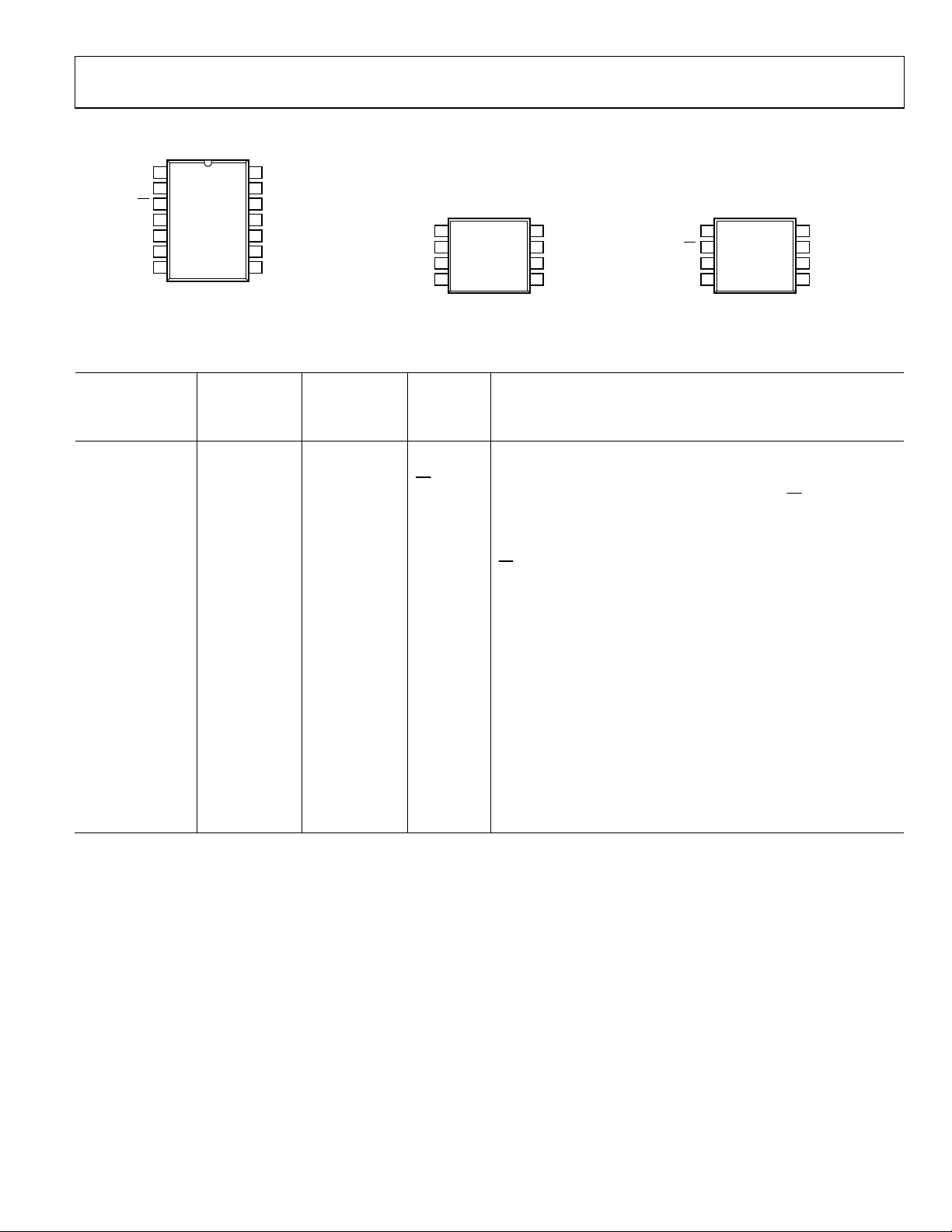
SOIC-14
描述:
3.3 V , 【 15千伏ESD保护,半双工和全双工, RS - 485 / RS -422收发器 3.3 V, 【15 kV ESD-Protected, Half- and Full-Duplex, RS-485/RS-422 Transceivers
Pictures:
3D模型
符号图
焊盘图
引脚图
产品图
页面导航:
导航目录
ADM3070EARZ-REEL7数据手册
Page:
of 20 Go
若手册格式错乱,请下载阅览PDF原文件
ADM3070E/ADM3071E/ADM3072E/ADM3073E/ADM3074E/ADM3075E/ADM3076E/ADM3077E/ADM3078E
Rev. E | Page 9 of 20
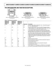
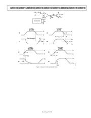
PIN CONFIGURATIONS AND FUNCTION DESCRIPTIONS
NC
1
RO
2
RE
3
DE
4
V
CC
14
NC
13
A
12
B
11
DI
5
Z
10
GND
6
Y
9
GND
7
NC
8
NC = NO CONNECT
ADM3070E/
ADM3073E/
ADM3076E
TOP VIEW
(Not to Scale)
06285-004
V
CC
1
RO
2
DI
3
GND
4
A
8
B
7
Z
6
Y
5
ADM3071E/
ADM3074E/
ADM3077E
TOP VIEW
(Not to Scale)
06285-005
RO
1
RE
2
DE
3
DI
4
V
CC
8
B
7
A
6
GND
5
ADM3072E/
ADM3075E/
ADM3078E
TOP VIEW
(Not to Scale)
06285-006
Figure 4. ADM3070E/ADM3073E/ADM3076E
Pin Configuration
Figure 5. ADM3071E/ADM3074E/ADM3077E
Pin Configuration
Figure 6. ADM3072E/ADM3075E/ADM3078E
Pin Configuration
Table 7. Pin Function Descriptions
ADM3070E/
ADM3073E/
ADM3076E
Pin No.
ADM3071E/
ADM3074E/
ADM3077E
Pin No.
ADM3072E/
ADM3075E/
ADM3078E
Pin No. Mnemonic Description
2 2 1 RO
Receiver Output. When enabled, if (A − B) ≥ −50 mV, RO is high. If
(A − B) ≤ −200 mV, RO is low.
3 N/A 2
RE
Receiver Output Enable. A low level enables the receiver output.
A high level places it in a high impedance state. If RE
is high and DE
is low, the device enters a low power shutdown mode.
4 N/A 3 DE
Driver Output Enable. A high level enables the driver differential
A and B outputs. A low level places it in a high impedance state. If
RE
is high and DE is low, the device enters a low power shutdown mode.
5 3 4 DI
Driver Input. With a half-duplex part when the driver is enabled, a
logic low on DI forces A low and B high; a logic high on DI forces
A high and B low. With a full-duplex part when the driver is enabled,
a logic low on DI forces Y low and Z high; a logic high on DI forces
Y high and Z low.
6, 7 4 5 GND
Ground.
9 5 N/A Y
Noninverting Driver Output.
N/A N/A 6 A
Noninverting Receiver Input A and Noninverting Driver Output A.
12 8 N/A A
Noninverting Receiver Input A.
10 6 N/A Z
Inverting Driver Output.
N/A N/A 7 B
Inverting Receiver Input B and Inverting Driver Output B.
11 7 N/A B
Inverting Receiver Input B.
14 1 8 V
CC
Power Supply, 3.3 V ± 10%. Bypass V
CC
to GND with a 0.1 μF capacitor.
1, 8, 13 N/A N/A NC No Connect. Not internally connected; can be connected to GND.
器件 Datasheet 文档搜索
AiEMA 数据库涵盖高达 72,405,303 个元件的数据手册,每天更新 5,000 多个 PDF 文件
