Datasheet 搜索 > 接口隔离器 > ADI(亚德诺) > ADM3260ARSZ 数据手册 > ADM3260ARSZ 数据手册 6/20 页
 器件3D模型
¥ 34.345
ADM3260ARSZ 数据手册 - ADI(亚德诺)
制造商:
ADI(亚德诺)
分类:
接口隔离器
封装:
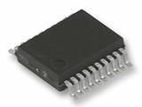
SSOP-20
描述:
ANALOG DEVICES ADM3260ARSZ 数字隔离器, 2通道, 3 V, 5.5 V, SSOP, 20 引脚
Pictures:
3D模型
符号图
焊盘图
引脚图
产品图
页面导航:
引脚图在P11Hot
典型应用电路图在P16
原理图在P1
封装尺寸在P19
型号编码规则在P19
封装信息在P6
功能描述在P1P11P15
技术参数、封装参数在P1P3P4P5P7P10P15
应用领域在P1P15P18
电气规格在P3P4P12
导航目录
ADM3260ARSZ数据手册
Page:
of 20 Go
若手册格式错乱,请下载阅览PDF原文件
ADM3260 Data Sheet
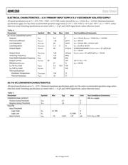
Parameter Symbol Min Typ Max Unit Test Conditions/Comments
Side 2 to Side 1
Rising Edge
3
t
PLH21
31 70 ns
Falling Edge
4
t
PHL21
85 155 ns
3 V Operation
3.0 V ≤ VDDISO, VDDP ≤ 3.6 V, C
L1
= C
L2
= 0 pF,
R1 = 1.0 kΩ, R2 = 120 Ω
Side 1 to Side 2
Rising Edge
1
t
PLH12
82 125 ns
Falling Edge
2
t
PHL12
196 340 ns
Side 2 to Side 1
Rising Edge
3
t
PLH21
32 75 ns
Falling Edge
4
t
PHL21
110
210
ns
PULSE WIDTH DISTORTION
5 V Operation
4.5 V ≤ VDDISO, VDDP ≤ 5.5 V, C
L1
= C
L2
= 0 pF,
R1 = 1.6 kΩ, R2 = 180 Ω
Side 1 to Side 2, |t
PLH12
− t
PHL12
| PWD
12
67 145 ns
Side 2 to Side 1, |t
PLH21
− t
PHL21
| PWD
21
54 85 ns
3 V Operation
3.0 V ≤ VDDISO, VDDP ≤ 3.6 V, C
L1
= C
L2
= 0 pF,
R1 = 1.0 kΩ, R2 = 120 Ω
Side 1 to Side 2, |t
PLH12
− t
PHL12
|
PWD
12
114
215
ns
Side 2 to Side 1, |t
PLH21
− t
PHL21
| PWD
21
77 135 ns
COMMON-MODE TRANSIENT IMMUNITY
5
|CM
H
|, |CM
L
| 25 35 kV/µs
1
t
PLH12
propagation delay is measured from the Side 1 input logic threshold to an output value of 0.7 VDDP.
2
t
PHL12
propagation delay is measured from the Side 1 input logic threshold to an output value of 0.4 V.
3
t
PLH21
propagation delay is measured from the Side 2 input logic threshold to an output value of 0.7 VDDISO.
4
t
PHL21
propagation delay is measured from the Side 2 input logic threshold to an output value of 0.9 V.
5
|CM
H
| is the maximum common-mode voltage slew rate that can be sustained while maintaining V
O
> 0.8 VDDP. |CM
L
| is the maximum common-mode voltage slew
rate that can be sustained while maintaining V
O
< 0.8 V. The common-mode voltage slew rates apply to both rising and falling common-mode voltage edges. The
transient magnitude is the range over which the common mode is slewed.
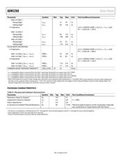
PACKAGE CHARACTERISTICS
Table 8. Thermal and Isolation Characteristics
Parameter Symbol Min Typ Max Unit Test Conditions/Comments
Resistance (Input to Output)
1
R
I-O
10
12
Ω
Capacitance (Input to Output)
1
C
I-O
2.2 pF f = 1 MHz
Input Capacitance
2
C
I
4.0 pF
IC Junction-to-Ambient Thermal Resistance θ
JA
50 °C/W
Thermocouple located at center of package underside,
test conducted on 4-layer board with thin traces
3
1
The device is considered a 2-terminal device: Pin 1 through Pin 10 are shorted together; and Pin 11 through Pin 20 are shorted together.
2
Input capacitance is from any input data pin to ground.
3
See the Thermal Analysis section for thermal model definitions.
Rev. A | Page 6 of 20
器件 Datasheet 文档搜索
AiEMA 数据库涵盖高达 72,405,303 个元件的数据手册,每天更新 5,000 多个 PDF 文件
