Datasheet 搜索 > 接口芯片 > ADI(亚德诺) > ADM3491EARZ-REEL7 数据手册 > ADM3491EARZ-REEL7 数据手册 15/20 页

 器件3D模型
¥ 2.286
ADM3491EARZ-REEL7 数据手册 - ADI(亚德诺)
制造商:
ADI(亚德诺)
分类:
接口芯片
封装:
SOIC-14
描述:
3.3 V , 【 15千伏ESD保护,半双工和全双工, RS - 485 / RS -422收发器 3.3 V, 【15 kV ESD-Protected, Half- and Full-Duplex, RS-485/RS-422 Transceivers
Pictures:
3D模型
符号图
焊盘图
引脚图
产品图
页面导航:
导航目录
ADM3491EARZ-REEL7数据手册
Page:
of 20 Go
若手册格式错乱,请下载阅览PDF原文件
ADM3483E/ADM3486E/ADM3488E/ADM3490E/ADM3491E
Rev. A | Page 15 of 20
±15 kV ESD PROTECTION
Two coupling methods are used for ESD testing: con-
tact discharge and air-gap discharge. Contact discharge
calls for a direct connection to the unit being tested. Air-
gap discharge uses a higher test voltage but does not make
direct contact with the test unit. With air-gap discharge,
the discharge gun is moved toward the unit under test,
developing an arc across the air gap, therefore the term air-
gap discharge. This method is influenced by humidity,
temperature, barometric pressure, distance, and rate of
closure of the discharge gun. The contact discharge
method, while less realistic, is more repeatable and is
gaining acceptance and preference over the air-
gap method.
Although very little energy is contained within an ESD pulse,
the extremely fast rise time, coupled with high voltages, can
cause failures in unprotected semiconductors. Catastrophic
destruction can occur immediately as a result of arcing or
heating. Even if catastrophic failure does not occur immediately,
the device can suffer from parametric degradation that can
result in degraded performance. The cumulative effects of
continuous exposure can eventually lead to complete failure.
Input/output lines are particularly vulnerable to ESD damage.
Simply touching or connecting an input/output cable can result
in a static discharge that can damage or completely destroy the
interface product connected to the input/output port. It is
extremely important, therefore, to have high levels of ESD
protection on the input/output lines.
The ESD discharge can induce latch-up in the device under test,
so it is important that ESD testing on the input/output pins be
carried out while device power is applied. This type of testing is
more representative of a real-world input/output discharge,
which occurs when the equipment is operating normally.
The transmitter outputs and receiver inputs of the ADM34xxE
family are characterized for protection to a ±15 kV limit using
the human body model.
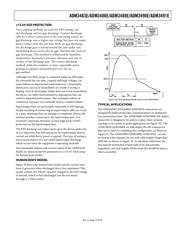
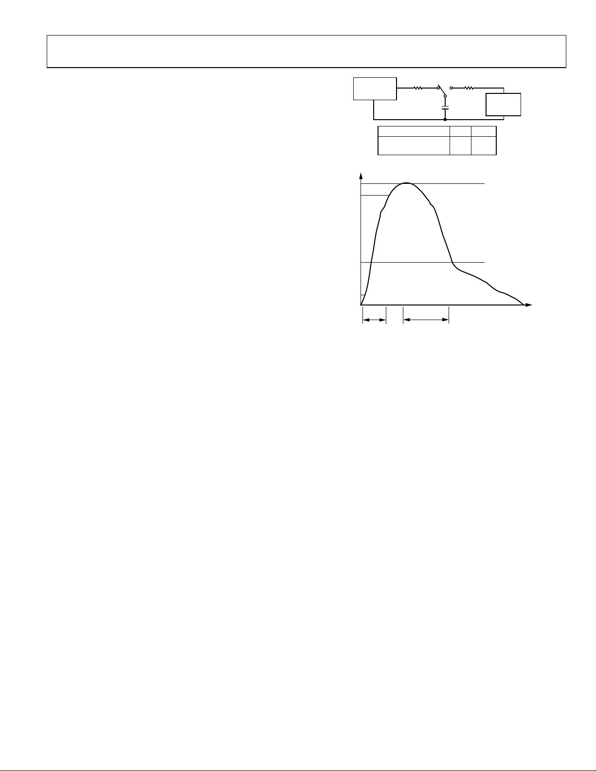
HUMAN BODY MODEL
Figure 30 shows the human body model and the current wave-
form it generates when discharged into a low impedance. This
model consists of a 100 pF capacitor charged to the ESD voltage
of interest, which is then discharged into the test device
through a 1.5 kΩ resistor.
100%
90%
36.8
%
10%
t
RL
t
DL
I
PEAK
TIME
t
R2
C1
R1
HIGH
VOLTAGE
GENERATOR
DEVICE
UNDER
TEST
ESD TEST METHOD
HUMAN BODY MODEL
ESD ASSOC. STD 55.1
R2
1.5k
C1
100pF
06284-016
Figure 30. Human Body Model and Current Waveform
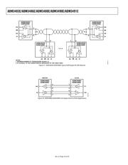
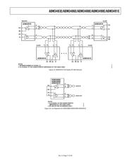
TYPICAL APPLICATIONS
The ADM3483E/ADM3486E/ADM3491E transceivers are
designed for bidirectional data communications on multipoint
bus transmission lines. The ADM3488E/ADM3490E full-duplex
transceiver is designed to be used in a daisy-chain network
topology or in a point-to-point application (see
Figure 32). The
ADM3483E/ADM3486E are half-duplex RS-485 transceivers
that can be used in a multidrop bus configuration, as shown in
Figure 31. The ADM3488E/ADM3490E/ADM3491E can also
be used as a line repeater, for use with cable lengths longer than
4000 feet, as shown in
Figure 34. To minimize reflections, the
line must be terminated at both ends in its characteristic
impedance, and stub lengths off the main line should be kept as
short as possible.
器件 Datasheet 文档搜索
AiEMA 数据库涵盖高达 72,405,303 个元件的数据手册,每天更新 5,000 多个 PDF 文件
