Datasheet 搜索 > 接口芯片 > ADI(亚德诺) > ADM485ANZ 数据手册 > ADM485ANZ 数据手册 1/16 页
 器件3D模型
¥ 41.04
ADM485ANZ 数据手册 - ADI(亚德诺)
制造商:
ADI(亚德诺)
分类:
接口芯片
封装:
DIP-8
描述:
RS-485 线路驱动器和接收器,Analog Devices### RS-485 线路驱动器和接收器
Pictures:
3D模型
符号图
焊盘图
引脚图
产品图
页面导航:
导航目录
ADM485ANZ数据手册
Page:
of 16 Go
若手册格式错乱,请下载阅览PDF原文件
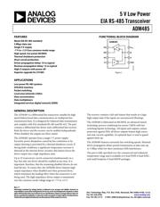
5 V Low Power
EIA RS-485 Transceiver
ADM485
Rev. F
Information furnished by Analog Devices is believed to be accurate and reliable. However, no
responsibility is assumed by Analog Devices for its use, nor for any infringements of patents or other
rights of third parties that may result from its use. Specifications subject to change without notice. No
license is granted by implication or otherwise under any patent or patent rights of Analog Devices.
Trademarks and registered trademarks are the property of their respective owners.
One Technology Way, P.O. Box 9106, Norwood, MA 02062-9106, U.S.A.
Tel: 781.329.4700 www.analog.com
Fax: 781.461.3113 ©1993–2008 Analog Devices, Inc. All rights reserved.
FEATURES
Meets EIA RS-485 standard
5 Mbps data rate
Single 5 V supply
–7 V to +12 V bus common-mode range
High speed, low power BiCMOS
Thermal shutdown protection
Short-circuit protection
Driver propagation delay: 10 ns typical
Receiver propagation delay: 15 ns typical
High-Z outputs with power off
Superior upgrade for LTC485
APPLICATIONS
Low power RS-485 systems
DTE/DCE interface
Packet switching
Local area networks (LNAs)
Data concentration
Data multiplexers
Integrated services digital network (ISDN)
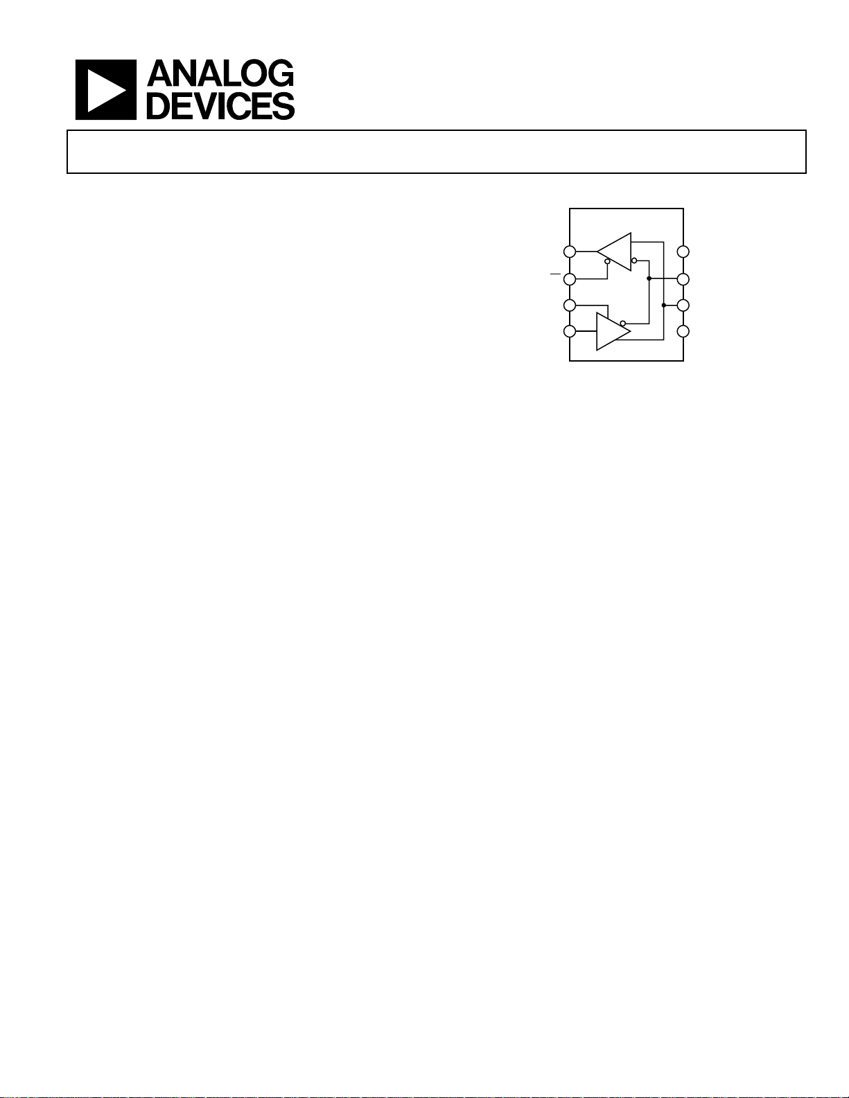
FUNCTIONAL BLOCK DIAGRAM
A
GND
B
V
CC
R
D
RO
RE
DE
DI
ADM485
00078-001
1
2
3
4
8
7
6
5
Figure 1.
GENERAL DESCRIPTION
The ADM485 is a differential line transceiver suitable for high
speed bidirectional data communication on multipoint bus
transmission lines. It is designed for balanced data transmission
and complies with EIA standards RS-485 and RS-422. The part
contains a differential line driver and a differential line receiver.
Both the driver and the receiver can be enabled independently.
When disabled, the outputs are three-stated.
The ADM485 operates from a single 5 V power supply.
Excessive power dissipation caused by bus contention or by
output shorting is prevented by a thermal shutdown circuit. If
during fault conditions, a significant temperature increase is
detected in the internal driver circuitry, this feature forces the
driver output into a high impedance state.
Up to 32 transceivers can be connected simultaneously on a
bus, but only one driver should be enabled at any time. It is
important, therefore, that the remaining disabled drivers do not
load the bus. To ensure this, the ADM485 driver features high
output impedance when disabled and when powered down,
which minimizes the loading effect when the transceiver is not
being used. The high impedance driver output is maintained
over the common-mode voltage range of −7 V to +12 V.
The receiver contains a fail-safe feature that results in a logic
high output state if the inputs are unconnected (floating).
The ADM485 is fabricated on BiCMOS, an advanced mixed
technology process combining low power CMOS with fast
switching bipolar technology. All inputs and outputs contain
protection against ESD; all driver outputs feature high source
and sink current capability. An epitaxial layer is used to guard
against latch-up.
The ADM485 features extremely fast switching speeds. Minimal
driver propagation delays permit transmission at data rates up
to 5 Mbps while low skew minimizes EMI interference.
The part is fully specified over the commercial and industrial
temperature range and is available in 8-lead PDIP, 8-lead SOIC,
and small footprint, 8-lead MSOP packages.
器件 Datasheet 文档搜索
AiEMA 数据库涵盖高达 72,405,303 个元件的数据手册,每天更新 5,000 多个 PDF 文件
