Datasheet 搜索 > ADI(亚德诺) > ADM802 数据手册 > ADM802 数据手册 6/8 页

 器件3D模型
¥ 0
ADM802 数据手册 - ADI(亚德诺)
制造商:
ADI(亚德诺)
封装:
SOIC
描述:
微处理器监控电路 Microprocessor Supervisory Circuits
Pictures:
3D模型
符号图
焊盘图
引脚图
产品图
页面导航:
导航目录
ADM802数据手册
Page:
of 8 Go
若手册格式错乱,请下载阅览PDF原文件
ADM690A/ADM692A/ADM802L/M/ADM805L/M
–6–
REV. 0
Table I. Input and Output Status in Battery Backup Mode
Signal Status
V
OUT
V
OUT
is connected to V
BATT
via an internal
PMOS switch.
RESET Logic low.
RESET Logic high (ADM805L, ADM805M). The open
circuit output voltage is equal to V
OUT
.
PFI The power fail comparator is disabled
PFO Logic low.
WDI The watchdog timer is disabled
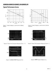
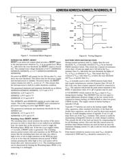
Power Fail Comparator
The power fail comparator is an independent comparator
that may be used to monitor the input power supply. The
comparator’s inverting input is internally connected to a 1.25
V reference voltage. The noninverting input is available at the
PFI input. This input may be used to monitor the input power
supply via a resistive divider network. When the voltage on the
PFI input drops below 1.25 V, the comparator output (
PFO)
goes low indicating a power failure. For early warning of power
failure the comparator may be used to monitor the preregulator
input simply by choosing an appropriate resistive divider
network. The
PFO output can be used to interrupt the
processor so that a shutdown procedure is implemented before
the power is lost.
1.25V
POWER FAIL
OUTPUT
(PFO)
POWER
FAIL
INPUT
INPUT
POWER
R1
R2
Figure 9. Power Fail Comparator
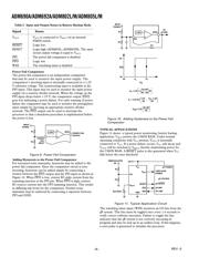
Adding Hysteresis to the Power Fail Comparator
For increased noise immunity, hysteresis may be added to the
power fail comparator. Since the comparator circuit is non-
inverting, hysteresis can be added simply by connecting a
resistor between the
PFO output and the PFI input as shown in
Figure 10. When
PFO is low, resistor R3 sinks current from the
summing junction at the PFI pin. When
PFO is high, resistor
R3 sources current into the PFI summing junction. This results
in differing trip levels for the comparator. Further noise
immunity may be achieved by connecting a capacitor between
PFI and GND.
1.25V
(PFO)
INPUT
POWER
R1
R2
PFI
R3
TO
µP NMI
5V
PFO
0V
0V V
L
V
H
V
IN
V
H
=
1.25
1
+ R
1
R
2
+R
3
R
2
×
R
3
V
L
= 1
.25
+R
1
1.25
V
CC
–
1.25
R
2
R
3
V
MID
=
1.25
R
1
+R
2
R
2
–
Figure 10. Adding Hysteresis to the Power Fail
Comparator
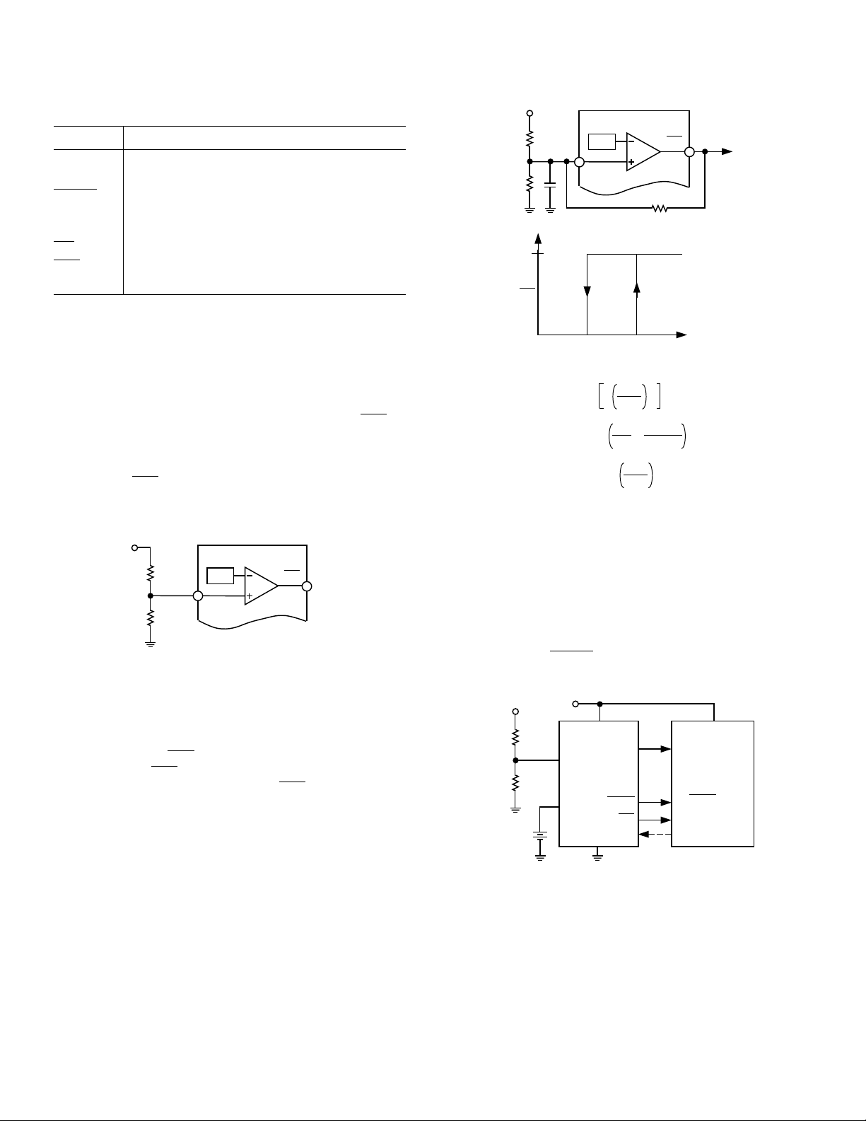
TYPICAL APPLICATIONS
Figure 11 shows a typical power monitoring, battery backup
application. V
OUT
powers the CMOS RAM. Under normal
operating conditions with V
CC
present, V
OUT
is internally
connected to V
CC
. If a power failure occurs, V
CC
will decay and
V
OUT
will be switched to V
BATT
thereby maintaining power for
the CMOS RAM. A
RESET pulse is also generated when V
CC
falls below the reset threshold.
CMOS RAM
POWER
µP RESET
µP NMI
I/O LINE
µP SYSTEM
V
CC
µP POWER
V
OUT
RESET
PFO
WDI
GND
V
BATT
PFI
UNREGULATED
DC
R1
R2
+5V
BATTERY
+
Figure 11. Typical Application Circuit
The watchdog timer input (WDI) monitors an I/O line from the
µP system. This line must be toggled once every 1.6 seconds to
verify correct software execution. Failure to toggle the line
indicates that the µP system is not correctly executing its
program and may be tied up in an endless loop. If this happens,
a reset pulse is generated to initialize the processor.
器件 Datasheet 文档搜索
AiEMA 数据库涵盖高达 72,405,303 个元件的数据手册,每天更新 5,000 多个 PDF 文件
