Datasheet 搜索 > DC/DC转换器 > ADI(亚德诺) > ADP5037ACPZ-R7 数据手册 > ADP5037ACPZ-R7 数据手册 2/28 页
 器件3D模型
¥ 22.533
ADP5037ACPZ-R7 数据手册 - ADI(亚德诺)
制造商:
ADI(亚德诺)
分类:
DC/DC转换器
封装:
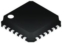
LFCSP-24
描述:
Analog DevicesAnalog Devices 的这些多输出调节器构成其电源管理系列的一部分。 此系列调节器提供完整的电源解决方案和高度集成的电源 IC。 这些设备实现可靠的电源解决方案,用于射频、高速和精密模拟产品,所有产品均采用紧凑型封装。 它们还特别适合用于 FPGA 和处理器。 Analog Devices 的多输出调节器具有 I²C 控制,可实现电压调节、排序和监控。 因此,它们可提高转换效率。它们结合以下功能,例如: \- 降压 \- 升压 \- 降压-升压开关调节器 \- 电池充电器 \- 自主背光控制 \- 低噪声 LDO 调节器 \- 实时时钟 ### 多输出稳压器,Analog Devices
Pictures:
3D模型
符号图
焊盘图
引脚图
产品图
页面导航:
引脚图在P7P27Hot
典型应用电路图在P1P25
原理图在P15P25
封装尺寸在P27
型号编码规则在P15P17P18P27
焊接温度在P6
功能描述在P1P7P27
技术参数、封装参数在P1P3P4P5P6
应用领域在P1P19P25
电气规格在P3P8

导航目录
ADP5037ACPZ-R7数据手册
Page:
of 28 Go
若手册格式错乱,请下载阅览PDF原文件

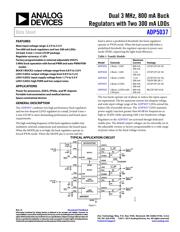
ADP5037 Data Sheet
Rev. D | Page 2 of 28
TABLE OF CONTENTS
Features .............................................................................................. 1
Applications ....................................................................................... 1
General Description ......................................................................... 1
Typical Application Circuit ............................................................. 1
Revision History ............................................................................... 2
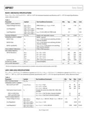
Specifications ..................................................................................... 3
General Specifications ................................................................. 3
BUCK1 and BUCK2 Specifications ........................................... 4
LDO1 and LDO2 Specifications ................................................. 4
Input and Output Capacitor, Recommended Specifications .. 5
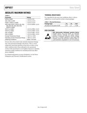
Absolute Maximum Ratings ............................................................ 6
Thermal Resistance ...................................................................... 6
ESD Caution .................................................................................. 6
Pin Configuration and Function Descriptions ............................. 7
Typical Performance Characteristics ............................................. 8
Theory of Operation ...................................................................... 15
Power Management Unit ........................................................... 15
BUCK1 and BUCK2 .................................................................. 17
LDO1 and LDO2 ........................................................................ 18
Applications Information .............................................................. 19
Buck External Component Selection ....................................... 19
LDO External Component Selection....................................... 21
Power Dissipation and Thermal Considerations ....................... 22
Buck Regulator Power Dissipation .......................................... 22
Junction Temperature ................................................................ 23
PCB Layout Guidelines .................................................................. 24
Typical Application Schematics .................................................... 25
Bill of Materials ............................................................................... 26
Outline Dimensions ....................................................................... 27
Ordering Guide .......................................................................... 27
REVISION HISTORY
5/13—Rev. C to Rev. D
Added Table 1; Renumbered Sequentially .................................... 1
Changes to Figure 1 .......................................................................... 1
Changes to NC Pin Description ..................................................... 7
Changes to Figure 48 ...................................................................... 18
Changes to Figure 50 ...................................................................... 20
Changes to Figure 52 and Figure 53 ............................................. 25
1/13—Rev. B to Rev. C
Changes to Figure 9 .......................................................................... 9
Changes to Ordering Guide .......................................................... 27
8/12—Rev. A to Rev. B
Changes to Regulator Accuracy, Features Section ....................... 1
Changes to Output Voltage Accuracy, Table 2 and Voltage
Feedback, Table 2 .............................................................................. 4
Changes to Output Voltage Accuracy, Table 3 and Voltage
Feedback, Table 3 .............................................................................. 4
Changes to Figure 6, Figure 7, and Figure 8.................................. 8
Changes to Figure 9 to Figure 14 .................................................... 9
Changes to Figure 30 and Figure 31 ............................................. 12
Changes to Figure 34 and Figure 38 Caption ............................. 13
Changes to Undervoltage Lockout Section ................................. 16
Moved Power Dissipation and Thermal Considerations
Section .............................................................................................. 22
Changes to Buck Regulator Power Dissipation Section ............ 22
Changes to PCB Layout Guidelines Section ............................... 24
Changes to Ordering Guide .......................................................... 27
1/12—Rev. 0 to Rev. A
Changes to Features Section and Figure 1 ..................................... 1
Changes to Table 2 and Table 3........................................................ 4
Changes to Table 4 ............................................................................. 5
Changes to Table 5 ............................................................................. 6
Changes to Table 7 ............................................................................. 7
Changes to Figure 34 ...................................................................... 13
Changes to Buck Regulator Power Dissipation Section ............ 15
Changes to Undervoltage Lockout Section ................................. 18
Changes to LDO1 and LDO2 Section ......................................... 20
Changes to Table 9 .......................................................................... 22
Changes to Figure 52 and Figure 53 ............................................ 25
Changes to Ordering Guide .......................................................... 27
8/11—Revision 0: Initial Version
器件 Datasheet 文档搜索
AiEMA 数据库涵盖高达 72,405,303 个元件的数据手册,每天更新 5,000 多个 PDF 文件
