Datasheet 搜索 > DC/DC转换器 > ADI(亚德诺) > ADP5037ACPZ-R7 数据手册 > ADP5037ACPZ-R7 数据手册 7/28 页
 器件3D模型
¥ 22.533
ADP5037ACPZ-R7 数据手册 - ADI(亚德诺)
制造商:
ADI(亚德诺)
分类:
DC/DC转换器
封装:
LFCSP-24
描述:
Analog DevicesAnalog Devices 的这些多输出调节器构成其电源管理系列的一部分。 此系列调节器提供完整的电源解决方案和高度集成的电源 IC。 这些设备实现可靠的电源解决方案,用于射频、高速和精密模拟产品,所有产品均采用紧凑型封装。 它们还特别适合用于 FPGA 和处理器。 Analog Devices 的多输出调节器具有 I²C 控制,可实现电压调节、排序和监控。 因此,它们可提高转换效率。它们结合以下功能,例如: \- 降压 \- 升压 \- 降压-升压开关调节器 \- 电池充电器 \- 自主背光控制 \- 低噪声 LDO 调节器 \- 实时时钟 ### 多输出稳压器,Analog Devices
Pictures:
3D模型
符号图
焊盘图
引脚图
产品图
页面导航:
引脚图在P7P27Hot
典型应用电路图在P1P25
原理图在P15P25
封装尺寸在P27
型号编码规则在P15P17P18P27
焊接温度在P6
功能描述在P1P7P27
技术参数、封装参数在P1P3P4P5P6
应用领域在P1P19P25
电气规格在P3P8
导航目录
ADP5037ACPZ-R7数据手册
Page:
of 28 Go
若手册格式错乱,请下载阅览PDF原文件
Data Sheet ADP5037
Rev. D | Page 7 of 28
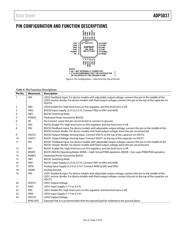
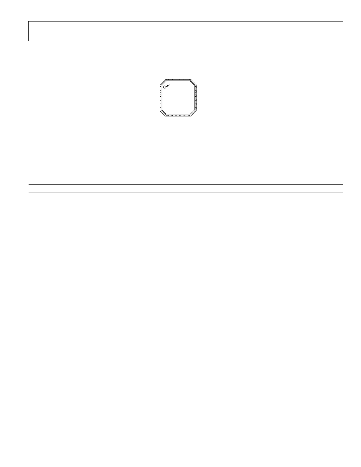
PIN CONFIGURATION AND FUNCTION DESCRIPTIONS
PIN 1
INDICATOR
NOTES
1. NC = NOT INTERNALLY CONNECTED.
2. IT IS RECOMMENDED THAT THE EXPOSED PAD
BE SOLDERED TO THE GROUND PLANE.
1
2
3
4
5
6
15
16
17
18
14
13
7
8
9
11
12
10
21
22
23
24
20
19
ADP5037
TOP VIEW
(Not to Scale)
VOUT4
FB3
VOUT3
VIN3
EN3
VIN4
AGND
AVIN
VIN1
SW1
PGND1
MODE
FB4
EN4
VIN2
SW2
PGND2
NC
EN1
FB1
VOUT1
VOUT2
FB2
EN2
09887-003
Figure 2. Pin Configuration—View from the Top of the Die
Table 8. Pin Function Descriptions
Pin No. Mnemonic Description
1 FB4 LDO2 Feedback Input. For device models with adjustable output voltage, connect this pin to the middle of the
LDO2 resistor divider. For device models with fixed output voltage, connect this pin to the top of the capacitor on
VOUT4.
2 EN4 LDO2 Enable Pin. High level turns on this regulator, and low level turns it off.
3
VIN2
BUCK2 Input Supply (2.3 V to 5.5 V). Connect VIN2 to VIN1 and AVIN.
4 SW2 BUCK2 Switching Node.
5 PGND2 Dedicated Power Ground for BUCK2.
6 NC No Connect. Leave this pin unconnected or connect to ground.
7 EN2 BUCK2 Enable Pin. High level turns on this regulator, and low level turns it off.
8 FB2 BUCK2 Feedback Input. For device models with adjustable output voltage, connect this pin to the middle of the
BUCK2 resistor divider. For device models with fixed output voltage, leave this pin unconnected.
9 VOUT2 BUCK2 Output Voltage Sensing Input. Connect VOUT2 to the top of the capacitor on VOUT2.
10 VOUT1 BUCK1 Output Voltage Sensing Input. Connect VOUT1 to the top of the capacitor on VOUT1.
11 FB1 BUCK1 Feedback Input. For device models with adjustable output voltage, connect this pin to the middle of the
BUCK1 resistor divider. For device models with fixed output voltage, leave this pin unconnected.
12
EN1
BUCK1 Enable Pin. High level turns on this regulator, and low level turns it off.
13 MODE BUCK1/BUCK2 Operating Mode. MODE = high: forced PWM operation. MODE = low: auto PWM/PSM operation.
14 PGND1 Dedicated Power Ground for BUCK1.
15 SW1 BUCK1 Switching Node.
16 VIN1 BUCK1 Input Supply (2.3 V to 5.5 V). Connect VIN1 to VIN2 and AVIN.
17 AVIN Analog Input Supply (2.3 V to 5.5 V). Connect AVIN to VIN1 and VIN2.
18 AGND Analog Ground.
19 FB3 LDO1 Feedback Input. For device models with adjustable output voltage, connect this pin to the middle of the
LDO1 resistor divider. For device models with fixed output voltage, connect this pin to the top of the capacitor on
VOUT3.
20 VOUT3 LDO1 Output Voltage.
21 VIN3 LDO1 Input Supply (1.7 V to 5.5 V).
22 EN3 LDO1 Enable Pin. High level turns on this regulator, and low level turns it off.
23 VIN4 LDO2 Input Supply (1.7 V to 5.5 V).
24 VOUT4 LDO2 Output Voltage.
EPAD (EP) Exposed Pad. It is recommended that the exposed pad be soldered to the ground plane.
器件 Datasheet 文档搜索
AiEMA 数据库涵盖高达 72,405,303 个元件的数据手册,每天更新 5,000 多个 PDF 文件
