Datasheet 搜索 > 稳压芯片 > ADI(亚德诺) > ADP7112ACBZ-1.2-R7 数据手册 > ADP7112ACBZ-1.2-R7 数据手册 1/22 页
 器件3D模型
¥ 7.511
ADP7112ACBZ-1.2-R7 数据手册 - ADI(亚德诺)
制造商:
ADI(亚德诺)
分类:
稳压芯片
封装:
WLCSP-6
描述:
20 V、200, m, A低噪声CMOS LDO线性稳压器
Pictures:
3D模型
符号图
焊盘图
引脚图
产品图
页面导航:
导航目录
ADP7112ACBZ-1.2-R7数据手册
Page:
of 22 Go
若手册格式错乱,请下载阅览PDF原文件
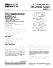
20 V, 200 mA, Low Noise,
CMOS LDO Linear Regulator
Data Sheet
ADP7112
Rev. C Document Feedback
Information furnished by Analog Devices is believed to be accurate and reliable. However, no
responsibility is assumed by Analog Devices for its use, nor for any infringements of patents or other
rights of third parties that may result from its use. Specifications subject to change without notice. No
license is granted by implication or otherwise under any patent or patent rights of Analog Devices.
Trademarks and registered trademarks are the property of their respective owners.
One Technology Way, P.O. Box 9106, Norwood, MA 02062-9106, U.S.A.
Tel: 781.329.4700 ©2014–2016 Analog Devices, Inc. All rights reserved.
Technical Support www.analog.com
FEATURES
Low noise: 11 µV rms independent of fixed output voltage
PSRR of 88 dB at 10 kHz, 68 dB at 100 kHz, 50 dB at 1 MHz,
V
OUT
= 5 V, V
IN
= 7 V
Input voltage range: 2.7 V to 20 V
Maximum output current: 200 mA
Initial accuracy: ±0.8%
Accuracy over line, load, and temperature
±1.8%, T
J
= −40°C to +125°C
Low dropout voltage: 200 mV (typical) at a 200 mA load,
V
OUT
= 5 V
User-programmable soft start
Low quiescent current, I
GND
= 50 μA (typical) with no load
Low shutdown current
1.8 μA at V
IN
= 5 V
3.0 μA at V
IN
= 20 V
Stable with a small 2.2 µF ceramic output capacitor
Fixed output voltage options: 1.8 V, 2.5 V, 3.3 V, and 5.0 V
15 standard voltages between 1.2 V and 5.0 V are available
Adjustable output from 1.2 V to V
IN
– V
DO
, output can be
adjusted above initial set point
Precision enable
1 mm × 1.2 mm, 6-ball WLCSP
APPLICATIONS
Regulation to noise sensitive applications
ADC and DAC circuits, precision amplifiers, power for
VCO V
TUNE
control
Communications and infrastructure
Medical and healthcare
Industrial and instrumentation
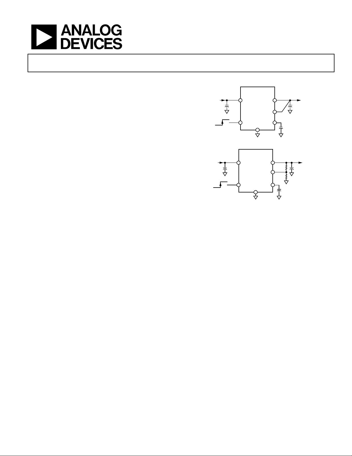
TYPICAL APPLICATION CIRCUITS
GND
EN
SS
VIN VOUT
ADP7112
ON
OFF
V
IN
= 6V V
OUT
= 5V
SENSE/ADJ
C
IN
2.2µF
C
OUT
2.2µF
C
SS
1nF
12508-001
Figure 1. ADP7112 with Fixed Output Voltage, 5 V
GND
EN SS
VIN VOUT
ADP7112
ON
OFF
V
IN
= 7V V
OUT
= 6V
SENSE/ADJ
C
IN
2.2µF
C
OUT
2.2µF
C
SS
1nF
2kΩ
10kΩ
12508-002
Figure 2. ADP7112 with 5 V Output Adjusted to 6 V
GENERAL DESCRIPTION
The ADP7112 is a CMOS, low dropout (LDO) linear regulator
that operates from 2.7 V to 20 V and provides up to 200 mA of
output current. This high input voltage LDO is ideal for the
regulation of high performance analog and mixed-signal circuits
operating from 20 V down to 1.2 V rails. Using an advanced
proprietary architecture, the device provides high power supply
rejection, low noise, and achieves excellent line and load transient
response with a small 2.2 µF ceramic output capacitor. The
ADP7112 regulator output noise is 11 μV rms, independent of
the output voltage for the fixed options of 5 V or less.
The ADP7112 is available in 15 fixed output voltage options.
The following voltages are available from stock: 1.2 V (adjustable),
1.8 V, 2.5 V, 3.3 V, and 5.0 V. Additional voltages available by
special order are 1.5 V, 1.85 V, 2.0 V, 2.2 V, 2.75 V, 2.8 V, 2.85 V,
3.8 V, 4.2 V, and 4.6 V.
Each fixed output voltage can be adjusted above the initial set
point with an external feedback divider. This allows the ADP7112
to provide an output voltage from 1.2 V to V
IN
− V
DO
with high
PSRR and low noise.
A user-programmable soft start with an external capacitor is
available in the ADP7112. The ADP7112 is available in a 6-ball
1 mm × 1.2 mm WLCSP, making it a very compact solution.
器件 Datasheet 文档搜索
AiEMA 数据库涵盖高达 72,405,303 个元件的数据手册,每天更新 5,000 多个 PDF 文件
