Datasheet 搜索 > 开发套件 > TI(德州仪器) > ADS4449EVM 数据手册 > ADS4449EVM 数据手册 21/56 页

¥ 5221.148
ADS4449EVM 数据手册 - TI(德州仪器)
制造商:
TI(德州仪器)
分类:
开发套件
Pictures:
3D模型
符号图
焊盘图
引脚图
产品图
页面导航:
引脚图在P3P4Hot
典型应用电路图在P41P42P43P44
原理图在P21
封装尺寸在P51P53P54
标记信息在P51
封装信息在P50P51P52P53P54
技术参数、封装参数在P5
应用领域在P1P56
电气规格在P7P8
导航目录
ADS4449EVM数据手册
Page:
of 56 Go
若手册格式错乱,请下载阅览PDF原文件
DAB0P, DAB0M or
OVRABP, OVRABM
CLKINP,
CLKINM
AINP,
AINM
Common
Mode
VCM
CLKOUTABP,
CLKOUTABM
DAB[13:1]P,
DAB[13:1]M
14
BINP,
BINM
CINP,
CINM
DINP,
DINM
Configuration Registers
CLKOUTCDP,
CLKOUTCDM
DCD[13:1]P,
DCD[13:1]M
14
Digital
Block
DCD0P, DCD0M or
OVRCDP, OVRCDM
Output
Formatter
DDR
LVDS
14-Bit
ADC
14-Bit
ADC
14-Bit
ADC
14-Bit
ADC
Digital
Block
SCLK
SEN
SDATA
SDOUT
RESET
PDN
21
ADS4449
www.ti.com
SBAS603A –APRIL 2013–REVISED JANUARY 2016
Product Folder Links: ADS4449
Submit Documentation FeedbackCopyright © 2013–2016, Texas Instruments Incorporated
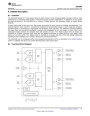
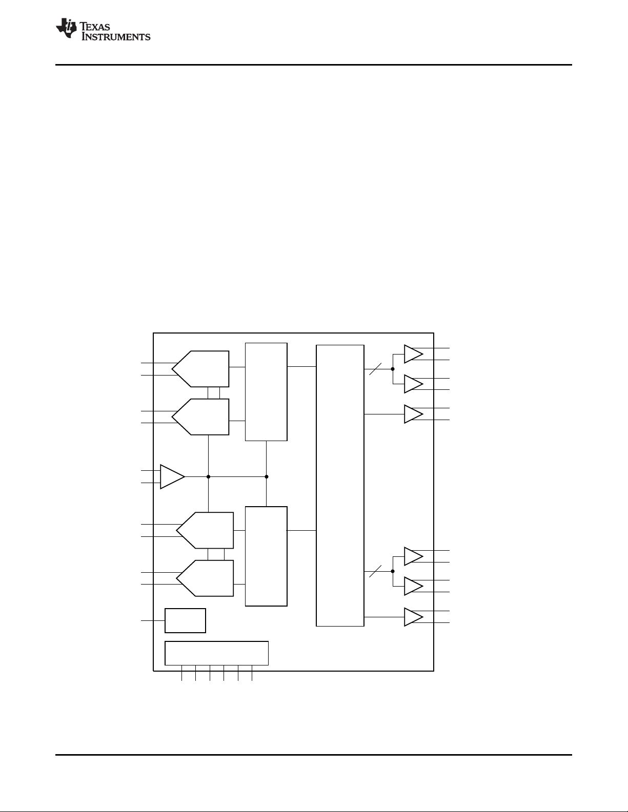
8 Detailed Description
8.1 Overview
The ADS4449 belong to TI’ s low-power family of quad-channel, 14-bit, analog-to-digital converters (ADCs). High
performance is maintained while power is reduced for power-sensitive applications. In addition to its low power
and high performance, the ADS4449 has a number of digital features and operating modes to enable design
flexibility.
At every falling edge of the input clock, the analog input signal for each channel is sampled simultaneously. The
sampled signal in each channel is converted by a pipeline of low-resolution stages. In each stage, the sampled-
and-held signal is converted by a high-speed, low-resolution, flash sub-ADC. The difference (residue) between
the stage input and quantized equivalent is gained and propagates to the next stage. At every clock, each
subsequent stage resolves the sampled input with greater accuracy. The digital outputs from all stages are
combined in a digital correction logic block and are digitally processed to create the final code, after a data
latency of 10 clock cycles. The digital output is available in a double data rate (DDR) low-voltage differential
signaling (LVDS) interface and is coded in binary twos complement format.
The ADS4449 can be configured with a serial programming interface (SPI), as described in the Serial Interface
section. In addition, the device has control terminals that control power-down.
8.2 Functional Block Diagram
器件 Datasheet 文档搜索
AiEMA 数据库涵盖高达 72,405,303 个元件的数据手册,每天更新 5,000 多个 PDF 文件
