Datasheet 搜索 > AD转换器 > TI(德州仪器) > ADS5547IRGZT 数据手册 > ADS5547IRGZT 数据手册 1/57 页

¥ 1121.799
ADS5547IRGZT 数据手册 - TI(德州仪器)
制造商:
TI(德州仪器)
分类:
AD转换器
封装:
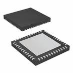
VQFN-48
描述:
14 - BIT , 210 MSPS的DDR LVDS / CMOS输出的ADC 14-BIT, 210 MSPS ADC WITH DDR LVDS/CMOS OUTPUTS
Pictures:
3D模型
符号图
焊盘图
引脚图
产品图
页面导航:
引脚图在P12P22P23P24P25Hot
封装尺寸在P50P52P53
型号编码规则在P2
标记信息在P2P50
封装信息在P2P50P51P52P53
技术参数、封装参数在P3P46P47P48
应用领域在P1P57
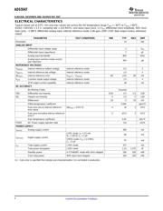
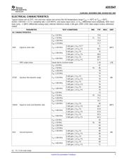
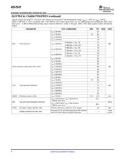
电气规格在P4P5P6
型号编号列表在P1
导航目录
ADS5547IRGZT数据手册
Page:
of 57 Go
若手册格式错乱,请下载阅览PDF原文件
www.ti.com
FEATURES DESCRIPTION
APPLICATIONS
ADS5547
SLWS192A – NOVEMBER 2006 – REVISED MAY 2007
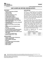
14-BIT, 210 MSPS ADC WITH DDR LVDS/CMOS OUTPUTS
• Maximum Sample Rate: 210 MSPS
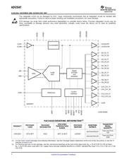
ADS5547 is a high performance 14-bit, 210-MSPS
A/D converter. It offers state-of-the art functionality
• 14-Bit Resolution
and performance using advanced techniques to
• No Missing Codes
minimize board space. With high analog bandwidth
• Total Power Dissipation 1.23 W
and low jitter input clock buffer, the ADC supports
• Internal Sample and Hold both high SNR and high SFDR at high input
frequencies. It features programmable gain options
• 73.3-dBFS SNR at 70-MHz IF
that can be used to improve SFDR performance at
• 85-dBc SFDR at 70-MHz IF, 0-dB gain
lower full-scale analog input ranges.
• High Analog Bandwidth up to 800 MHz
In a compact 48-pin QFN, the device offers fully
• Double Data Rate (DDR) LVDS and Parallel
differential LVDS DDR (Double Data Rate) interface
CMOS Output Options
while parallel CMOS outputs can also be selected.
Flexible output clock position programmability is
• Programmable Gain up to 6 dB for SNR/SFDR
available to ease capture and trade-off setup for hold
Trade-Off at High IF
times. At lower sampling rates, the ADC can be
• Reduced Power Modes at Lower Sample
operated at scaled down power with no loss in
Rates
performance. The ADS5547 includes an internal
• Supports Input Clock Amplitude Down to
reference, while eliminating the traditional reference
400 mV
PP
pins and associated external decoupling. The device
also supports an external reference mode.
• Clock Duty Cycle Stabilizer
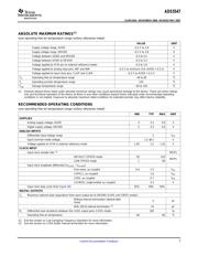
The device is specified over the industrial
• No External Reference Decoupling Required
temperature range (-40 ° C to 85 ° C).
• Internal and External Reference Support
• Programmable Output Clock Position to Ease
ADS5547 PRODUCT FAMILY
Data Capture
210 MSPS 190 MSPS 170 MSPS
• 3.3-V Analog and Digital Supply
14 bit ADS5547 ADS5546 ADS5545
• 48-QFN Package (7 mm × 7 mm)
12 bit ADS5527 - ADS5525
• Wireless Communications Infrastructure
• Software Defined Radio
• Power Amplifier Linearization
• 802.16d/e
• Test and Measurement Instrumentation
• High Definition Video
• Medical Imaging
• Radar Systems
Please be aware that an important notice concerning availability, standard warranty, and use in critical applications of Texas
Instruments semiconductor products and disclaimers thereto appears at the end of this data sheet.
PRODUCTION DATA information is current as of publication date.
Copyright © 2006–2007, Texas Instruments Incorporated
Products conform to specifications per the terms of the Texas
Instruments standard warranty. Production processing does not
necessarily include testing of all parameters.
器件 Datasheet 文档搜索
AiEMA 数据库涵盖高达 72,405,303 个元件的数据手册,每天更新 5,000 多个 PDF 文件
