Datasheet 搜索 > AD转换器 > TI(德州仪器) > ADS6142IRHB25 数据手册 > ADS6142IRHB25 数据手册 1/67 页

¥ 0
ADS6142IRHB25 数据手册 - TI(德州仪器)
制造商:
TI(德州仪器)
分类:
AD转换器
封装:
VFQFN-32
Pictures:
3D模型
符号图
焊盘图
引脚图
产品图
页面导航:
引脚图在P21P22P23P24Hot
封装尺寸在P60P62P63
型号编码规则在P3
标记信息在P3
封装信息在P3P60P61P62P63
技术参数、封装参数在P3P56
应用领域在P1P67
电气规格在P5P6P7
导航目录
ADS6142IRHB25数据手册
Page:
of 67 Go
若手册格式错乱,请下载阅览PDF原文件
1
FEATURES
DESCRIPTION
APPLICATIONS
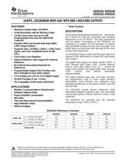
ADS6145, ADS6144
ADS6143, ADS6142
SLWS198B – JULY 2007 – REVISED MARCH 2008
www.ti.com
14-BITS, 125/105/80/65 MSPS ADC WITH DDR LVDS/CMOS OUTPUTS
• Radar Systems
• Maximum Sample Rate: 125 MSPS
• 14-Bit Resolution with No Missing Codes
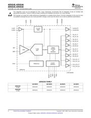
ADS6145/ADS6144/ADS6143/ADS6142 (ADS614X)
• 3.5 dB Coarse Gain and up to 6 dB
are a family of 14-bit A/D converters with sampling
Programmable Fine Gain for SNR/SFDR
frequencies up to 125 MSPS. The high performance
Trade-Off
and low power consumption of the ADS614X are
• Parallel CMOS and Double Data Rate (DDR)
combined in a compact 32 QFN package. An internal
LVDS Output Options
high bandwidth sample and hold and a low jitter clock
buffer help to achieve high SNR and high SFDR even
• Supports Sine, LVCMOS, LVPECL, LVDS Clock
at high input frequencies.
Inputs, and Clock Amplitude Down to 400
mV
PP The ADS614X feature coarse and fine gain options to
improve SFDR performance at lower full-scale analog
• Clock Duty Cycle Stabilizer
input ranges.
• Internal Reference with Support for External
Reference
The digital data outputs are either parallel CMOS or
DDR (Double Data Rate) LVDS. Several features
• No External Decoupling Required for
exist to ease data capture such as — controls for
References
output clock position and output buffer drive strength,
• Programmable Output Clock Position and
LVDS current, and internal termination
Drive Strength to Ease Data Capture
programmability.
• 3.3-V Analog and 1.8-V to 3.3-V Digital Supply
The output interface type, gain, and other functions
• 32-QFN Package (5 mm × 5 mm)
are programmed using a 3-wire serial interface.
Alternatively, some functions are configured using
• Pin Compatible 12-Bit Family (ADS612X)
dedicated parallel pins so the device powers up to the
desired state.
The ADS614X include internal references while
• Wireless Communications Infrastructure
eliminating traditional reference pins and associated
• Software Defined Radio
external decoupling. External reference mode is also
• Power Amplifier Linearization
supported.
• 802.16d/e
The ADS614X are specified over the industrial
• Test and Measurement Instrumentation
temperature range ( – 40 ° C to 85 ° C).
• High Definition Video
• Medical Imaging
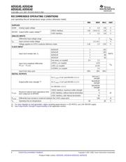
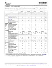
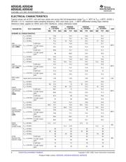
ADS614X Performance Summary
ADS6145 ADS6144 ADS6143 ADS6142
F
in
= 10 MHz (0 dB gain) 90 91 93 95
SFDR, dBc
F
in
= 170 MHz (3.5 dB gain) 78 82 83 84
F
in
= 10 MHz (0 dB gain) 73.7 74.1 74.5 74.6
SINAD, dBFS
F
in
= 170 MHz (3.5 dB gain) 68.6 70.5 70.6 71.5
Power, mW 417 374 318 285
1
Please be aware that an important notice concerning availability, standard warranty, and use in critical applications of
Texas Instruments semiconductor products and disclaimers thereto appears at the end of this data sheet.
PRODUCTION DATA information is current as of publication date.
Copyright © 2007 – 2008, Texas Instruments Incorporated
Products conform to specifications per the terms of the Texas
Instruments standard warranty. Production processing does not
necessarily include testing of all parameters.
器件 Datasheet 文档搜索
AiEMA 数据库涵盖高达 72,405,303 个元件的数据手册,每天更新 5,000 多个 PDF 文件
