Datasheet 搜索 > AD转换器 > TI(德州仪器) > ADS8320E/250 数据手册 > ADS8320E/250 数据手册 13/21 页
 器件3D模型
¥ 49.524
ADS8320E/250 数据手册 - TI(德州仪器)
制造商:
TI(德州仪器)
分类:
AD转换器
封装:
VSSOP-8
描述:
TEXAS INSTRUMENTS ADS8320E/250 模数转换器, 16 bit, 100 kSPS, 单, 2.7 V, 5.25 V, VSSOP
Pictures:
3D模型
符号图
焊盘图
引脚图
产品图
页面导航:
导航目录
ADS8320E/250数据手册
Page:
of 21 Go
若手册格式错乱,请下载阅览PDF原文件
ADS8320
13
SBAS108D
www.ti.com
The basic SAR architecture is sensitive to spikes on the
power supply, reference, and ground connections that occur
just prior to latching the comparator output. Thus, during
any single conversion for an n-bit SAR converter, there are
n “windows” in which large external transient voltages can
easily affect the conversion result. Such spikes might origi-
nate from switching power supplies, digital logic, and high
power devices, to name a few. This particular source of error
can be very difficult to track down if the glitch is almost
synchronous to the converter DCLOCK signal—as the phase
difference between the two changes with time and tempera-
ture, causing sporadic misoperation.
With this in mind, power to the ADS8320 should be clean
and well bypassed. A 0.1µF ceramic bypass capacitor should
be placed as close to the ADS8320 package as possible. In
addition, a 1µF to 10µF capacitor and a 5Ω or 10Ω series
resistor may be used to low-pass filter a noisy supply.
The reference should be similarly bypassed with a 0.1µF
capacitor. Again, a series resistor and large capacitor can be
used to low-pass filter the reference voltage. If the reference
voltage originates from an op amp, be careful that the op
amp can drive the bypass capacitor without oscillation (the
series resistor can help in this case). Keep in mind that while
the ADS8320 draws very little current from the reference on
average, there are still instantaneous current demands placed
on the external input and reference circuitry.
Texas Instruments' OPA627 op amp provides optimum
performance for buffering both the signal and reference
inputs. For low-cost, low-voltage, single-supply applica-
tions, the OPA2350 or OPA2340 dual op amps are recom-
mended.
Also, keep in mind that the ADS8320 offers no inherent
rejection of noise or voltage variation in regards to the
reference input. This is of particular concern when the
reference input is tied to the power supply. Any noise and
ripple from the supply will appear directly in the digital
results. While high-frequency noise can be filtered out as
described in the previous paragraph, voltage variation due to
the line frequency (50Hz or 60Hz), can be difficult to
remove.
The GND pin on the ADS8320 should be placed on a clean
ground point. In many cases, this will be the “analog”
ground. Avoid connecting the GND pin too close to the
grounding point for a microprocessor, microcontroller, or
digital signal processor. If needed, run a ground trace di-
rectly from the converter to the power-supply connection
point. The ideal layout includes an analog ground plane for
the converter and associated analog circuitry.
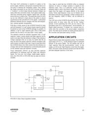
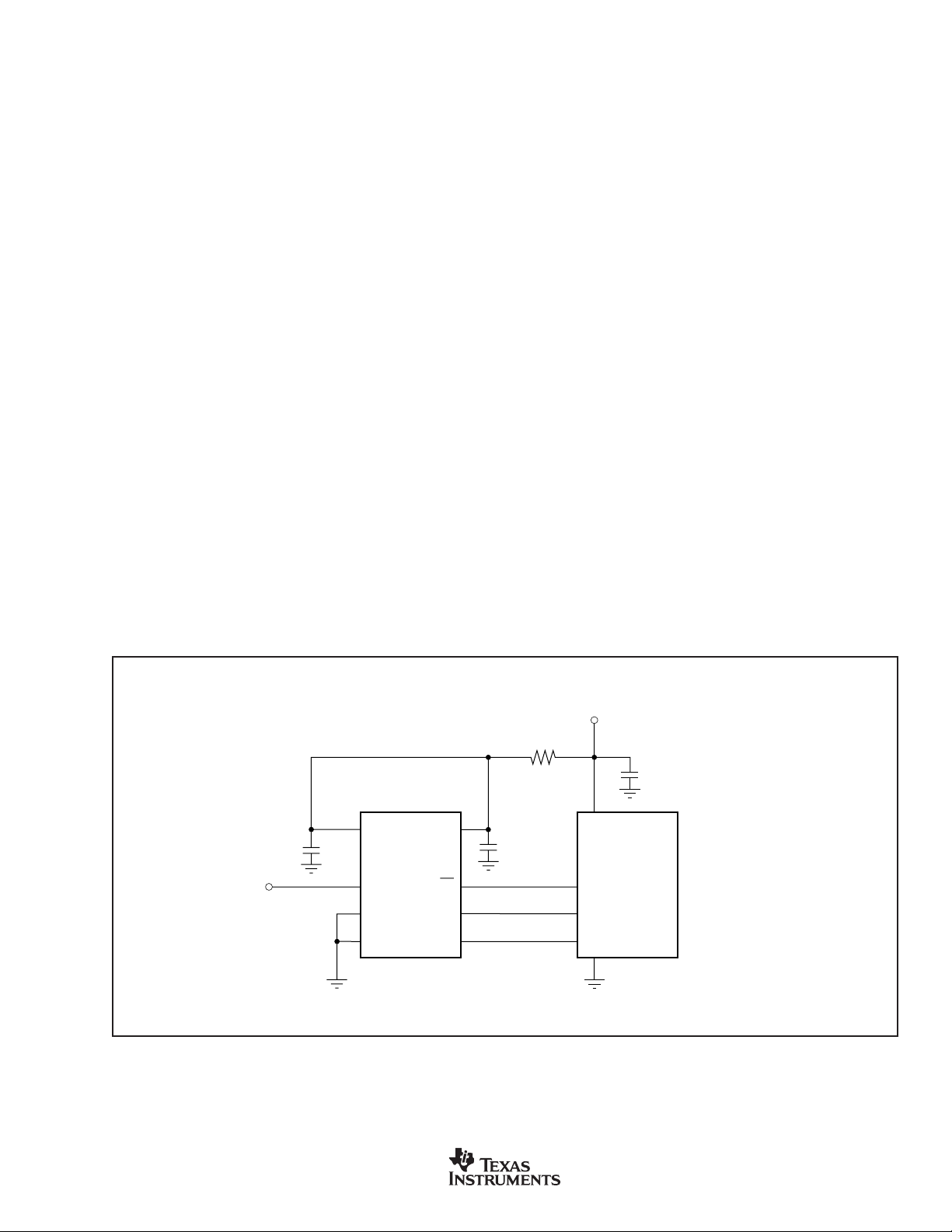
APPLICATION CIRCUITS
Figure 8 shows a basic data acquisition system. The ADS8320
input range is 0V to V
CC
, as the reference input is connected
directly to the power supply. The 5Ω resistor and 1µF to
10µF capacitor filter the microcontroller “noise” on the
supply, as well as any high-frequency noise from the supply
itself. The exact values should be picked such that the filter
provides adequate rejection of the noise.
FIGURE 8. Basic Data Acquisition System.
ADS8320
V
CC
CS
D
OUT
DCLOCK
V
REF
+In
–In
GND
+
+
5Ω
1µF to
10µF
1µF to
10µF
0.1µF
Microcontroller
+2.7V to +5.25V
器件 Datasheet 文档搜索
AiEMA 数据库涵盖高达 72,405,303 个元件的数据手册,每天更新 5,000 多个 PDF 文件
