Datasheet 搜索 > Burr Brown > ADS8325 数据手册 > ADS8325 数据手册 5/21 页


¥ 0
ADS8325 数据手册 - Burr Brown
制造商:
Burr Brown
Pictures:
3D模型
符号图
焊盘图
引脚图
产品图
页面导航:
导航目录
ADS8325数据手册
Page:
of 21 Go
若手册格式错乱,请下载阅览PDF原文件
ADS8325
5
SBAS226A
www.ti.com
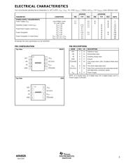
PIN CONFIGURATION
NAME PIN I/O DESCRIPTION
REF 1 AI Reference Input
+IN 2 AI Noninverting Input
–IN 3 AI Inverting Analog Input
GND 4 P Ground
CS/SHDN 5 DI Chip Select when LOW, Shutdown Mode when
HIGH.
D
OUT
6 DO The serial output data word.
DCLOCK 7 DI Data Clock synchronizes the serial data transfer
and determines conversion speed.
V
DD
8 P Power Supply
NOTE: AI is Analog Input, DI is Digital Input, DO is Digital Output, and P is
Power-Supply Connection.
Top View MSOP
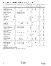
ELECTRICAL CHARACTERISTICS
Over recommended operating free-air temperature at –40°C to 85°C, V
REF
= V
DD
, –IN = GND, f
SAMPLE
= 100kHz, and f
CLK
= 24 • f
SAMPLE
, unless otherwise noted.
ADS8325I ADS8325IB
PARAMETER CONDITIONS MIN TYP MAX MIN TYP MAX UNITS
POWER-SUPPLY REQUIREMENTS
Power Supply (V
DD)
Low-Voltage Levels 2.7 3.6 ✻✻V
5V Logic Levels 4.5 5.5 ✻✻V
Operating Supply Current (I
DD
)V
DD
= 3V 0.75 1.5 ✻✻mA
V
DD
= 5V 0.9 1.5 ✻✻mA
Power-Down Supply Current (I
DD
)V
DD
= 3V 0.1 ✻ µA
V
DD
= 5V 0.2 ✻ µA
Power Dissipation V
DD
= 3V 2.25 4.5 ✻✻mW
V
DD
= 5V 4.5 7.5 ✻✻mW
Power Dissipation in Power-Down V
DD
= 3V, CS = V
DD
0.3 ✻ µW
V
DD
= 5V, CS = V
DD
0.6 ✻ µW
✻ indicates the same specifications as the ADS8325I.
1
2
3
4
8
7
6
5
+V
DD
DCLOCK
D
OUT
CS/SHDN
REF
+IN
–IN
GND
ADS8325
PIN DESCRIPTIONS
1
2
3
4
8
7
6
5
+V
DD
DCLOCK
D
OUT
CS/SHDN
REF
+IN
–IN
GND
ADS8325
Top View SON
器件 Datasheet 文档搜索
AiEMA 数据库涵盖高达 72,405,303 个元件的数据手册,每天更新 5,000 多个 PDF 文件
