Datasheet 搜索 > 微控制器 > ADI(亚德诺) > ADUC7021BCPZ62-RL 数据手册 > ADUC7021BCPZ62-RL 数据手册 1/101 页
 器件3D模型
¥ 84.007
ADUC7021BCPZ62-RL 数据手册 - ADI(亚德诺)
制造商:
ADI(亚德诺)
分类:
微控制器
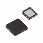
封装:
LFCSP-40
描述:
精密模拟微控制器, 12位模拟I / O , ARM7TDMI MCU Precision Analog Microcontroller, 12-Bit Analog I/O, ARM7TDMI MCU
Pictures:
3D模型
符号图
焊盘图
引脚图
产品图
页面导航:
引脚图在P21P22P23P25P26P28P31P33P68P97Hot
原理图在P1P9P85P86P87P88
封装尺寸在P97
焊盘布局在P94
型号编码规则在P1P4P9P47P96P100
焊接温度在P20
功能描述在P4P21P23P26P28P31P33P68P97
技术参数、封装参数在P1P10P13P20P38P50
应用领域在P1
电气规格在P35
导航目录
ADUC7021BCPZ62-RL数据手册
Page:
of 101 Go
若手册格式错乱,请下载阅览PDF原文件
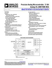
Precision Analog Microcontroller, 12-Bit
Analog I/O, ARM7TDMI MCU
Data Sheet
ADuC7019/20/21/22/24/25/26/27/28/29
Rev. G Document Feedback
Information furnished by Analog Devices is believed to be accurate and reliable. However, no
responsibility is assumed by Analog Devices for its use, nor for any infringements of patents or other
rights of third parties that may result from its use. Specifications subject to change without notice. No
license is granted by implication or otherwise under any patent or patent rights of Analog Devices.
Trademarks and registered trademarks are the property of their respective owners.
One Technology Way, P.O. Box 9106, Norwood, MA 02062-9106, U.S.A.
Tel: 781.329.4700 ©2005–2015 Analog Devices, Inc. All rights reserved.
Technical Support www.analog.com
FEATURES
Analog I/O
Multichannel, 12-bit, 1 MSPS ADC
Up to 16 ADC channels
1
Fully differential and single-ended modes
0 V to V
REF
analog input range
12-bit voltage output DACs
Up to 4 DAC outputs available
1
On-chip voltage reference
On-chip temperature sensor (±3°C)
Voltage comparator
Microcontroller
ARM7TDMI core, 16-bit/32-bit RISC architecture
JTAG port supports code download and debug
Clocking options
Trimmed on-chip oscillator (±3%)
External watch crystal
External clock source up to 44 MHz
41.78 MHz PLL with programmable divider
Memory
62 kB Flash/EE memory, 8 kB SRAM
In-circuit download, JTAG-based debug
Software-triggered in-circuit reprogrammability
On-chip peripherals
UART, 2× I
2
C® and SPI serial I/O
Up to 40-pin GPIO port
1
4× general-purpose timers
Wake-up and watchdog timers (WDT)
Power supply monitor
3-phase, 16-bit PWM generator
1
Programmable logic array (PLA)
External memory interface, up to 512 kB
1
Power
Specified for 3 V operation
Active mode: 11 mA @ 5 MHz, 40 mA @ 41.78 MHz
Packages and temperature range
From 40-lead 6 mm × 6 mm LFCSP to 80-lead LQFP
1
Fully specified for –40°C to +125°C operation
Tools
Low cost QuickStart™ development system
Full third-party support
APPLICATIONS
Industrial control and automation systems
Smart sensors, precision instrumentation
Base station systems, optical networking
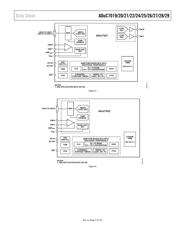
FUNCTIONAL BLOCK DIAGRAM
1MSPS
12-BIT ADC
DAC0
12-BIT
DAC
DAC1
DAC2
3-PHASE
PWM
(SEE NOTE 1)
ADuC7019
ADC0 TO ADC4,
A
DC12 TO ADC14
XCLKI
XCLKO
RST
V
REF
MUX
TEMP
SENSOR
BAND GAP
REF
OSC
AND PLL
PSM
POR
CMP0
CMP1
CMP
OUT
PLA
4 GENERAL-
PURPOSE TIMERS
2k × 32 SRAM
31k × 16 FLASH/EEPROM
SERIAL I/O
UART, SPI, I
2
C
GPIO
JTAG
ARM7TDMI-BASED MCU WITH
ADDITIONAL PERIPHERALS
12-BIT
DAC
12-BIT
DAC
NOTES
1. SEE APPLICATION NOTE AN-798.
ADC15
04955-100
Figure 1.
1
Depending on part model. See Ordering Guide for more information.
器件 Datasheet 文档搜索
AiEMA 数据库涵盖高达 72,405,303 个元件的数据手册,每天更新 5,000 多个 PDF 文件
