Datasheet 搜索 > MOS管 > Alpha & Omega Semiconductor(万代半导体) > AON7934 数据手册 > AON7934 数据手册 6/10 页
 器件3D模型
¥ 0.683
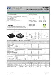
AON7934 数据手册 - Alpha & Omega Semiconductor(万代半导体)
制造商:
Alpha & Omega Semiconductor(万代半导体)
分类:
MOS管
封装:
WDFN-8
描述:
二极管与整流器
Pictures:
3D模型
符号图
焊盘图
引脚图
产品图
页面导航:
功能描述在P1
技术参数、封装参数在P1
应用领域在P2P6
电气规格在P2P6
导航目录
AON7934数据手册
Page:
of 10 Go
若手册格式错乱,请下载阅览PDF原文件
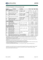
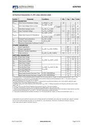
AON7934
Symbol Min Typ Max Units
BV
DSS
30 V
V
DS
=30V, V
GS
=0V 1
T
J
=55°C 5
I
GSS
100 nA
V
GS(th)
Gate Threshold Voltage
1.2 1.8 2.2 V
6.3 7.7
T
J
=125°C 8.4 10.3
9.1 11.6 mΩ
g
FS
100 S
V
SD
0.7 1 V
I
S
18 A
C
iss
807 pF
C
oss
314 pF
C
rss
40 pF
R
g
0.6 1.3 2 Ω
Q
g
(10V) 12.9 17.5 nC
Q
g
(4.5V) 6 8.5 nC
Q
gs
2.1 nC
Q
gd
3 nC
t
D(on)
4.8 ns
t
r
3.3 ns
t
18.8
ns
Maximum Body-Diode Continuous Current
G
Input Capacitance
Output Capacitance
Turn-On DelayTime
DYNAMIC PARAMETERS
Turn-On Rise Time
Turn-Off DelayTime
V
GS
=10V, V
DS
=15V, R
L
=1Ω,
R
=3
Ω
Gate resistance
V
GS
=0V, V
DS
=0V, f=1MHz
Total Gate Charge
I
S
=1A,V
GS
=0V
Gate Source Charge
Gate Drain Charge
V
GS
=10V, V
DS
=15V, I
D
=15A
Reverse Transfer Capacitance
I
D
=250µA, V
GS
=0V
Diode Forward Voltage
V
DS
=V
GS
I
D
=250µA
V
DS
=0V, V
GS
= ±20V
Gate-Body leakage current
Static Drain-Source On-Resistance
I
DSS
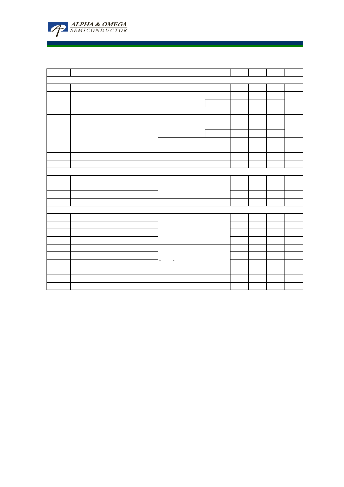
Q2 Electrical Characteristics (T
J
=25°C unless otherwise noted)
STATIC PARAMETERS
Parameter Conditions
Drain-Source Breakdown Voltage
Zero Gate Voltage Drain Current
µA
R
DS(ON)
mΩ
V
DS
=5V, I
D
=15A
V
GS
=0V, V
DS
=15V, f=1MHz
SWITCHING PARAMETERS
Total Gate Charge
Forward Transconductance
V
GS
=4.5V, I
D
=10A
V
GS
=10V, I
D
=15A
t
D(off)
18.8
ns
t
f
3.3 ns
t
rr
11.3 ns
Q
rr
15
nC
COMPONENTS IN LIFE SUPPORT DEVICES OR SYSTEMS ARE NOT AUTHORIZED. AOS DOES NOT ASSUME ANY LIABILITY ARISING
OUT OF SUCH APPLICATIONS OR USES OF ITS PRODUCTS. AOS RESERVES THE RIGHT TO IMPROVE PRODUCT DESIGN,
FUNCTIONS AND RELIABILITY WITHOUT NOTICE.
Body Diode Reverse Recovery Charge
I
F
=15A, dI/dt=500A/µs
Turn-Off DelayTime
R
GEN
=3
Ω
Turn-Off Fall Time
I
F
=15A, dI/dt=500A/µs
Body Diode Reverse Recovery Time
A. The value of R
θJA
is measured with the device mounted on 1in
2
FR-4 board with 2oz. Copper, in a still air environment with T
A
=25°C. The
Power dissipation P
DSM
is based on R
θJA
t≤ 10s value and the maximum allowed junction temperature of 150°C. The value in any given
application depends on the user's specific board design.
B. The power dissipation P
D
is based on T
J(MAX)
=150°C, using junction-to-case thermal resistance, and is more useful in setting the upper
dissipation limit for cases where additional heatsinking is used.
C. Repetitive rating, pulse width limited by junction temperature T
J(MAX)
=150°C. Ratings are based on low frequency and duty cycles to keep
initial T
J
=25°C.
D. The R
θJA
is the sum of the thermal impedence from junction to case R
θJC
and case to ambient.
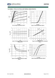
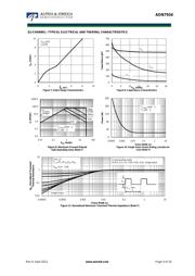
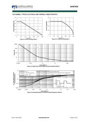
E. The static characteristics in Figures 1 to 6 are obtained using <300µs pulses, duty cycle 0.5% max.
F. These curves are based on the junction-to-case thermal impedence which is measured with the device mounted to a large heatsink, assuming
a maximum junction temperature of T
J(MAX)
=150°C. The SOA curve provides a single pulse rating.
G. These tests are performed with the device mounted on 1 in
2
FR-4 board with 2oz. Copper, in a still air environment with T
A
=25°C.
Rev 0: April 2012 www.aosmd.com Page 6 of 10
器件 Datasheet 文档搜索
AiEMA 数据库涵盖高达 72,405,303 个元件的数据手册,每天更新 5,000 多个 PDF 文件
