Datasheet 搜索 > 存储芯片 > Adesto Technologies > AT45DB041E-SHN2B-T 数据手册 > AT45DB041E-SHN2B-T 数据手册 6/70 页
 器件3D模型
¥ 4.357
AT45DB041E-SHN2B-T 数据手册 - Adesto Technologies
制造商:
Adesto Technologies
分类:
存储芯片
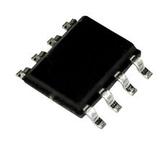
封装:
SOIC-8
描述:
闪存, 串行NOR, 4 Mbit, SPI, WSOIC, 8 引脚
Pictures:
3D模型
符号图
焊盘图
引脚图
产品图
页面导航:
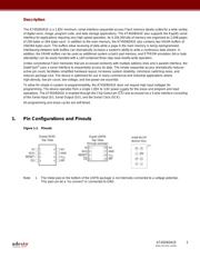
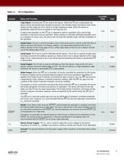
引脚图在P2P3P68Hot
原理图在P4P54P55
封装尺寸在P65P66P67P68
型号编码规则在P35P63P64
封装信息在P63P65
技术参数、封装参数在P46
应用领域在P27
电气规格在P46
型号编号列表在P63
导航目录
AT45DB041E-SHN2B-T数据手册
Page:
of 70 Go
若手册格式错乱,请下载阅览PDF原文件
6
AT45DB041E
8783I–DFLASH–3/2016
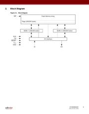
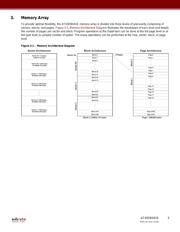
4. Device Operation
The device operation is controlled by instructions from the host processor. The list of instructions and their associated
opcodes are contained in Table 15-1 on page 40 through Table 15-4 on page 41. A valid instruction starts with the falling
edge of CS
followed by the appropriate 8-bit opcode and the desired buffer or main memory address location. While the
CS
pin is low, toggling the SCK pin controls the loading of the opcode and the desired buffer or main memory address
location through the SI (Serial Input) pin. All instructions, addresses, and data are transferred with the Most Significant
Bit (MSB) first.
Three address bytes are used to address memory locations in either the main memory array or in one of the SRAM
buffers. The three address bytes will be comprised of a number of dummy bits and a number of actual device address
bits, with the number of dummy bits varying depending on the operation being performed and the selected device page
size. Buffer addressing for the standard DataFlash page size (264 bytes) is referenced in the datasheet using the
terminology BFA8 - BFA0 to denote the 9 address bits required to designate a byte address within a buffer. The main
memory addressing is referenced using the terminology PA10 - PA0 and BA8 - BA0, where PA10 - PA0 denotes the
11 address bits required to designate a page address, and BA8 - BA0 denotes the 9 address bits required to designate a
byte address within the page. Therefore, when using the standard DataFlash page size, a total of 20 address bits are
used.
For the “power of 2” binary page size (256 bytes), the buffer addressing is referenced in the datasheet using the
conventional terminology BFA7 - BFA0 to denote the eight address bits required to designate a byte address within a
buffer. Main memory addressing is referenced using the terminology A18 - A0, where A18 - A8 denotes the 11 address
bits required to designate a page address, and A7 - A0 denotes the eight address bits required to designate a byte
address within a page. Therefore, when using the binary page size, a total of 19 address bits are used.
器件 Datasheet 文档搜索
AiEMA 数据库涵盖高达 72,405,303 个元件的数据手册,每天更新 5,000 多个 PDF 文件
