Datasheet 搜索 > ATMEL(爱特美尔) > AT88SC118-SH-CM 数据手册 > AT88SC118-SH-CM 数据手册 5/36 页

 器件3D模型
¥ 5.548
AT88SC118-SH-CM 数据手册 - ATMEL(爱特美尔)
制造商:
ATMEL(爱特美尔)
封装:
SOIC-8
描述:
安全IC/验证IC CryptoMemory Comp 8SOIC, GRN
Pictures:
3D模型
符号图
焊盘图
引脚图
产品图
页面导航:
导航目录
AT88SC118-SH-CM数据手册
Page:
of 36 Go
若手册格式错乱,请下载阅览PDF原文件

5
Atmel AT88SC118 [DATASHEET]
Atmel-8857A-CryptoComp-AT88SC118-Datasheet_052013
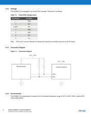
1.4.5 TWI Input/Output Operation
The AT88SC118 communicates to the system using a 2-Wire Interface (TWI), which is similar to SMBus
™
. The chip
operates as a slave and does not support clock stretching. This 2-Wire protocol is identical to that supported by the Atmel
AT24C16B Serial EEPROM chips. Refer to the datasheet on the Atmel website for detailed timing and protocol
information.
The system processor is expected to properly format commands for the AT88SC118 (which may include information
from the CRF chip), and then process the outputs of the AT88SC118 (which may include sending some of the outputs to
the CRF chip).
The AT88SC118 cannot directly communicate with CRF or CM chips. Both CRF/CM and the
AT88SC118 are slave devices. The bus master may use one or two busses to communicate with them. Separate TWI
addresses must be used if both chips are on the same bus.
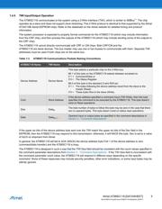
Table 1-3. AT88SC118 Communications Packets Naming Conventions.
If the upper six bits of the device address byte sent over the TWI match the upper six bits of the Dev field in the
EEPROM, then the AT88SC118 may respond to this transmission; otherwise, it will NACK this byte. Dev is set to a value
of 0xC0 on shipment from Atmel.
In general, the AT88SC118 will fail to ACK (NACK) the device address byte if bit 1 of the device address is zero
(command/data transfer) and the AT88SC118 is busy.
The AT88SC118 is designed in such a way that the TWI Size field should be consistent with the count values specified in
the command parameter descriptions from Section 3., “Command Descriptions”. If the TWI Size field is inconsistent with
the command parameter count value, the AT88SC118 will respond in different ways depending on the specific
command. Some of these responses may include security penalties, other error indications, or some input bytes may be
silently ignored.
AT88SC118 Name TWI Name Description
Device Address Device Name
This byte selects a particular chip on the 2-Wire bus.
Bit 1 of this byte on the AT88SC118 selects between accesses to:
If 1 = Command/Data or
If 0 = The Status Register.
Bit 0 of this byte is the standard 2-wire R/W pin.
If 1 = The bytes following the device address travel from the slave to the
master (Read).
If 0 = These bytes flow to the slave (Write).
Cmd Word Address
If the device address specified a command input (TWI Write), then this byte
specifies the command to be executed by the AT88SC118. This byte doesn’t
exist on Read operations.
Size Data
N
The total number of bytes to follow this byte may be zero in the case that there
are no operand bytes. This byte doesn’t exist on status read operations.
Data Data
N+1
, …
Operand input or output bytes as specified in the command descriptions in
Section 3., “Command Descriptions”
器件 Datasheet 文档搜索
AiEMA 数据库涵盖高达 72,405,303 个元件的数据手册,每天更新 5,000 多个 PDF 文件
