Datasheet 搜索 > 8位微控制器 > ATMEL(爱特美尔) > ATTINY13A-SSU 数据手册 > ATTINY13A-SSU 数据手册 51/176 页
 器件3D模型
¥ 7.3
ATTINY13A-SSU 数据手册 - ATMEL(爱特美尔)
制造商:
ATMEL(爱特美尔)
分类:
8位微控制器
封装:
SOIC-8
描述:
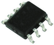
ATMEL ATTINY13A-SSU 微控制器, 8位, 低功率高性能, ATtiny, 20 MHz, 1 KB, 60 Byte, 8 引脚, SOIC
Pictures:
3D模型
符号图
焊盘图
引脚图
产品图
页面导航:
引脚图在P2P3P51Hot
原理图在P4P7P49P59P61P62P63P79P82
封装尺寸在P163P164P165P166P167
型号编码规则在P162
封装信息在P163
应用领域在P28
电气规格在P96P162
导航目录
ATTINY13A-SSU数据手册
Page:
of 176 Go
若手册格式错乱,请下载阅览PDF原文件

51
8126F–AVR–05/12
ATtiny13A
If PORTxn is written logic one when the pin is configured as an input pin, the pull-up resistor is
activated. To switch the pull-up resistor off, PORTxn has to be written logic zero or the pin has to
be configured as an output pin. The port pins are tri-stated when reset condition becomes active,
even if no clocks are running.
If PORTxn is written logic one when the pin is configured as an output pin, the port pin is driven
high (one). If PORTxn is written logic zero when the pin is configured as an output pin, the port
pin is driven low (zero).
10.2.2 Toggling the Pin
Writing a logic one to PINxn toggles the value of PORTxn, independent on the value of DDRxn.
Note that the SBI instruction can be used to toggle one single bit in a port.
10.2.3 Switching Between Input and Output
When switching between tri-state ({DDxn, PORTxn} = 0b00) and output high ({DDxn, PORTxn}
= 0b11), an intermediate state with either pull-up enabled {DDxn, PORTxn} = 0b01) or output
low ({DDxn, PORTxn} = 0b10) must occur. Normally, the pull-up enabled state is fully accept-
able, as a high-impedant environment will not notice the difference between a strong high driver
and a pull-up. If this is not the case, the PUD bit in the MCUCR Register can be set to disable all
pull-ups in all ports.
Switching between input with pull-up and output low generates the same problem. The user
must use either the tri-state ({DDxn, PORTxn} = 0b00) or the output high state ({DDxn, PORTxn}
= 0b10) as an intermediate step.
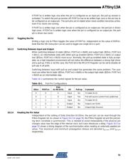
Table 10-1 summarizes the control signals for the pin value.
10.2.4 Reading the Pin Value
Independent of the setting of Data Direction bit DDxn, the port pin can be read through the
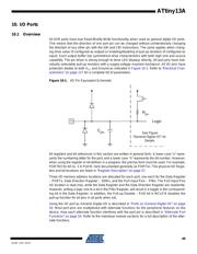
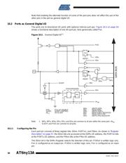
PINxn Register bit. As shown in Figure 10-2 on page 50, the PINxn Register bit and the preced-
ing latch constitute a synchronizer. This is needed to avoid metastability if the physical pin
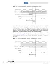
changes value near the edge of the internal clock, but it also introduces a delay. Figure 10-3 on
page 52 shows a timing diagram of the synchronization when reading an externally applied pin
value. The maximum and minimum propagation delays are denoted t
pd,max
and t
pd,min
respectively.
Table 10-1. Port Pin Configurations
DDxn PORTxn
PUD
(in MCUCR) I/O Pull-up Comment
0 0 X Input No Tri-state (Hi-Z)
0 1 0 Input Yes Pxn will source current if ext. pulled low.
0 1 1 Input No Tri-state (Hi-Z)
1 0 X Output No Output Low (Sink)
1 1 X Output No Output High (Source)
器件 Datasheet 文档搜索
AiEMA 数据库涵盖高达 72,405,303 个元件的数据手册,每天更新 5,000 多个 PDF 文件
