Datasheet 搜索 > 8位微控制器 > ON Semiconductor(安森美) > AX8052F143-2-TX30 数据手册 > AX8052F143-2-TX30 数据手册 2/45 页
 器件3D模型
¥ 14.929
AX8052F143-2-TX30 数据手册 - ON Semiconductor(安森美)
制造商:
ON Semiconductor(安森美)
分类:
8位微控制器
封装:
QFN-40
描述:
27 Mhz 至 1.05 GHz 125 kbps 16 dbm 64 kB 闪存 8 kB SRAM RF 微控制器 SoC
Pictures:
3D模型
符号图
焊盘图
引脚图
产品图
页面导航:
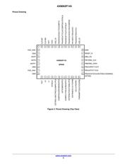
引脚图在P4P5Hot
典型应用电路图在P32P34P35P36P37P38P39P40P41
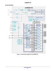
原理图在P3P23P25
封装尺寸在P42
焊盘布局在P44
型号编码规则在P45
标记信息在P45
功能描述在P4
技术参数、封装参数在P7
应用领域在P1P2P13
型号编号列表在P7
导航目录
AX8052F143-2-TX30数据手册
Page:
of 45 Go
若手册格式错乱,请下载阅览PDF原文件

AX8052F143
www.onsemi.com
2
♦
Sensitivity with FEC
−137 dBm @ 0.1 kbps, 868 MHz, FSK
−122 dBm @ 5 kbps, 868 MHz, FSK
−111 dBm @ 50 kbps, 868 MHz, FSK
♦ High Selectivity Receiver with up to 47 dB Adjacent
Channel Rejection
♦ 0 dBm Maximum Input Power
♦ ±10% Data−rate Error Tolerance
♦ Support for Antenna Diversity with External
Antenna Switch
♦ Short Preamble Modes allow the Receiver to work
with as little as 16 Preamble Bits
♦ Fast State Switching Times
200 ms TX → RX Switching Time
62 ms RX → TX Switching Time
• Transmitter
♦ Carrier Frequencies from 27 to 1050 MHz
♦ Data−rates from 0.1 kbps to 125 kbps
♦ High Efficiency, High Linearity Integrated Power
Amplifier
♦ Maximum Output Power
16 dBm @ 868 MHz
16 dBm @ 433 MHz
16 dBm @ 169 MHz
♦ Power Level programmable in 0.5 dB Steps
♦ GFSK Shaping with BT=0.3 or BT=0.5
♦ Unrestricted Power Ramp Shaping
• RF Frequency Generation
♦ Configurable for Usage in 27 MHz −1050 MHz
Bands
♦ RF Carrier Frequency and FSK Deviation
Programmable in 1 Hz Steps
♦ Ultra Fast Settling RF Frequency Synthesizer for
Low−power Consumption
♦ Fully Integrated RF Frequency Synthesizer with
VCO Auto−ranging and Band−width Boost Modes
for Fast Locking
♦ Configurable for either Fully Integrated VCO,
Internal VCO with External Inductor or Fully
External VCO
♦ Configurable for either Fully Integrated or External
Synthesizer Loop Filter for a Large Range of
Bandwidths
♦ Channel Hopping up to 2000 hops/s
♦ Automatic Frequency Control (AFC)
• Flexible Antenna Interface
♦ Integrated RX/TX Switching with Differential
Antenna Pins
♦ Mode with Differential RX Pins and Single−ended
TX Pin for Usage with External PAs and for
Maximum PA Efficiency at Low Output Power
• Wakeup−on−Radio
♦ 640 Hz or 10 kHz Lowest Power Wake−up Timer
♦ Wake−up Time Interval programmable between
98 ms and 102 s
• Sophisticated Radio Controller
♦ Antenna Diversity and RX/TX Switch Control
♦ Fully Automatic Packet Reception and Transmission
without Micro−controller Intervention
♦ Supports HDLC, Raw, Wireless M−Bus Frames and
Arbitrary Defined Frames
♦ Automatic Channel Noise Level Tracking
♦ ms Resolution Timestamps for Exact Timing (eg. for
Frequency Hopping Systems)
♦ 256 Byte Micro−programmable FIFO, optionally
supports Packet Sizes > 256 Bytes
♦ Three Matching Units for Preamble Byte,
Sync−word and Address
♦ Ability to store RSSI, Frequency Offset and
Data−rate Offset with the Packet Data
♦ Multiple Receiver Parameter Sets allow the use of
more aggressive Receiver Parameters during
Preamble, dramatically shortening the Required
Preamble Length at no Sensitivity Degradation
• Advanced Crystal Oscillator (RF Reference Oscillator)
♦ Fast Start−up and Lowest Power Steady−state XTAL
Oscillator for a Wide Range of Crystals
♦ Integrated Tuning Capacitors
♦ Possibility of Applying an External Clock Reference
(TCXO)
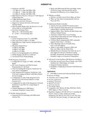
Applications
27 − 1050 MHz Licensed and Unlicensed Radio Systems
• Internet of Things
• Automatic meter reading (AMR)
• Security applications
• Building automation
• Wireless networks
• Messaging Paging
• Compatible with: Wireless M−Bus, POCSAG, FLEX,
KNX, Sigfox, Z−Wave, enocean
• Regulatory Regimes: EN 300 220 V2.3.1 including the
Narrow−band 12.5 kHz, 20 kHz and 25 kHz
Definitions; EN 300 422; FCC Part 15.247; FCC Part
15.249; FCC Part 90 6.25 kHz, 12.5 kHz and 25 kHz
器件 Datasheet 文档搜索
AiEMA 数据库涵盖高达 72,405,303 个元件的数据手册,每天更新 5,000 多个 PDF 文件
