Datasheet 搜索 > 电池管理芯片 > TI(德州仪器) > BQ24157SYFFR 数据手册 > BQ24157SYFFR 数据手册 6/45 页
¥ 927.748
BQ24157SYFFR 数据手册 - TI(德州仪器)
制造商:
TI(德州仪器)
分类:
电池管理芯片
封装:
UFBGA-20
描述:
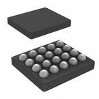
与 USB 完全兼容的全集成式开关模式单节锂离子充电器,bq24157S 20-DSBGA
Pictures:
3D模型
符号图
焊盘图
引脚图
产品图
页面导航:
引脚图在P3Hot
典型应用电路图在P1P29
原理图在P12P13P14
封装尺寸在P40P42P43
标记信息在P40
封装信息在P39P40P41P42P43
技术参数、封装参数在P4
应用领域在P1P45
电气规格在P5P6P7P8P9P10
型号编号列表在P30
导航目录
BQ24157SYFFR数据手册
Page:
of 45 Go
若手册格式错乱,请下载阅览PDF原文件

Not Recommended for New Designs
bq24157S
SLUSB76B –FEBRUARY 2013–REVISED MAY 2015
www.ti.com
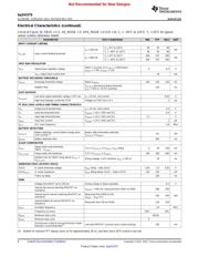
Electrical Characteristics (continued)
Circuit of Figure 28, VBUS = 5 V, HZ_MODE = 0, OPA_MODE = 0 (CD = 0), T
J
= –40°C to 125°C, T
J
= 25°C for typical
values (unless otherwise noted)
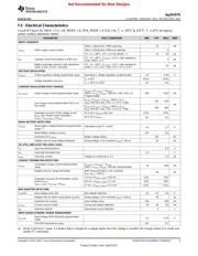
PARAMETER TEST CONDITIONS MIN TYP MAX UNIT
INPUT CURRENT LIMITING
T
J
= 0°C to 125°C 88 93 98
I
IN
= 100 mA mA
T
J
= –40°C to 125°C 86 93 98
I
IN_LIMIT
Input current limiting threshold
T
J
= 0°C to 125°C 450 475 500
I
IN
= 500 mA mA
T
J
= –40°C to 125°C 440 475 500
VREF BIAS REGULATOR
VBUS > V
IN
(min) or V
(CSOUT)
> VBUS(min),
V
REF
Internal bias regulator voltage 2 6.5 V
I
(VREF)
= 1 mA, C
(VREF)
= 1 μF
V
REF
output short current limit 30 mA
BATTERY RECHARGE THRESHOLD
V
(RCH)
Recharge threshold voltage Below V
(OREG)
100 120 150 mV
V
(SCOUT)
decreasing below threshold,
Deglitch time 130 ms
t
FALL
= 100 ns, 10-mV overdrive
STAT OUTPUTS
Low-level output saturation voltage, STAT pin I
O
= 10 mA, sink current 0.55 V
V
OL(STAT)
High-level leakage current for STAT Voltage on STAT pin is 5 V 1 μA
I
2
C BUS LOGIC LEVELS AND TIMING CHARACTERISTICS
V
OL
Output low threshold level I
O
= 10 mA, sink current 0.4 V
V
IL
Input low threshold level V
(pullup)
= 1.8 V, SDA and SCL 0.4 V
V
IH
Input high threshold level V
(pullup)
= 1.8 V, SDA and SCL 1.2 V
I
(BIAS)
Input bias current V
(pullup)
= 1.8 V, SDA and SCL 1 μA
f
(SCL)
SCL clock frequency 3.4 MHz
BATTERY DETECTION
Battery detection current before charge done Begins after termination detected,
I
(DETECT)
–0.5 mA
(sink current)
(2)
V
(CSOUT)
≤ V
(OREG)
t
DETECT
Battery detection time 262 ms
SLEEP COMPARATOR
Sleep-mode entry threshold,
V
(SLP)
2.3 V ≤ V
(CSOUT)
≤ V
(OREG)
, V
BUS
falling 0 40 100 mV
VBUS – V
CSOUT
V
(SLP_EXIT)
Sleep-mode exit hysteresis 2.3 V ≤ V
(CSOUT)
≤ V
(OREG)
140 200 260 mV
Deglitch time for VBUS rising above V
(SLP)
+
Rising voltage, 2-mV overdrive, t
RISE
= 100 ns 30 ms
V
(SLP_EXIT)
UNDERVOLTAGE LOCKOUT (UVLO)
UVLO IC active threshold voltage V
BUS
rising – exits UVLO 3.05 3.3 3.55 V
UVLO
(HYS)
IC active hysteresis V
BUS
falling below UVLO – enters UVLO 120 150 mV
Power up delay 140 ms
PWM
Voltage from BOOT pin to SW pin During charge or boost operation 6.5 V
Internal top reverse blocking MOSFET on-
I
IN(LIMIT)
= 500 mA, measured from VBUS to PMID 180 250
resistance
Internal top N-channel switching MOSFET on- Measured from PMID to SW,
120 250 mΩ
resistance V
BOOT
– V
SW
= 4 V
Internal bottom N-channel MOSFET on-
Measured from SW to PGND 110 210
resistance
f
(OSC)
Oscillator frequency 3.0 MHz
Frequency accuracy –10% 10%
D
(MAX)
Maximum duty cycle 99.5%
D
(MIN)
Minimum duty cycle 0
Synchronous mode to non-synchronous mode
Low-side MOSFET cycle-by-cycle current sensing 100 mA
transition current threshold
(2)
(2) Bottom N-channel FET always turns on for approximately 30 ns, and then turns off if current is too low.
6 Submit Documentation Feedback Copyright © 2013–2015, Texas Instruments Incorporated
Product Folder Links: bq24157S
器件 Datasheet 文档搜索
AiEMA 数据库涵盖高达 72,405,303 个元件的数据手册,每天更新 5,000 多个 PDF 文件

