Datasheet 搜索 > 电池管理芯片 > TI(德州仪器) > BQ24250YFFR 数据手册 > BQ24250YFFR 数据手册 3/58 页
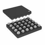
 器件3D模型
¥ 17.046
BQ24250YFFR 数据手册 - TI(德州仪器)
制造商:
TI(德州仪器)
分类:
电池管理芯片
封装:
UFBGA-30
描述:
2A单输入I2C ,独立开关模式锂离子电池充电器与电源路径管理 2A Single Input I2C, Standalone Switch-Mode Li-Ion Battery Charger with Power-Path Management
Pictures:
3D模型
符号图
焊盘图
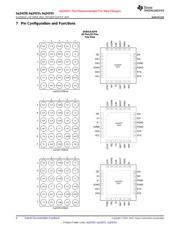
引脚图
产品图
页面导航:
引脚图在P6P7P8Hot
典型应用电路图在P40P41
原理图在P18
封装尺寸在P48P50P51P55
焊盘布局在P56
标记信息在P48P49
封装信息在P9P46P48P49P50P51
技术参数、封装参数在P9
应用领域在P1P58
电气规格在P10P11P12P13P14
导航目录
BQ24250YFFR数据手册
Page:
of 58 Go
若手册格式错乱,请下载阅览PDF原文件

bq24250
,
bq24251
,
bq24253
www.ti.com
SLUSBA1H –OCTOBER 2012–REVISED AUGUST 2015
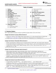
• Changed text string in the Input Over-Voltage Protection description from: "...turns the battery FET, sends a single
256μs pulse is sent on the STAT and INT outputs..." to "...turns the battery FET, sends a single 256μs pulse on the
STAT and INT outputs...."..................................................................................................................................................... 26
• Added Serial Interface Description....................................................................................................................................... 31
• Changed Register #3 description, B1(4)(5) Name from: "USB_DET_1/EN1" to: "USB_DET_1/EN2" ................................ 35
• Changed Register #3 description, B0(LSB) Name from: "USB_DET_0/EN0" to: "USB_DET_0/EN1"................................ 35
• Changed Register #3 description, B1(4)(5) and B0(LSB) FUNCTION entries from: "Return USB detection result or
pin EN1/EN0 status –" to "Return USB detection result or pin EN2/EN1 status –" ; changed 00 - DCP detected /
from: "EN1=0, EN0=0" to: "EN2=0, EN1=0"; changed 01 - CDP detected / from: "EN1=0, EN0=1 " to: "EN2=0,
EN1=1"; changed 10 - SDP detected / from: "EN1=1, EN0=0" to: "EN2=1, EN1=0"; and changed 11 - Apple/TT or
non-standard adaptor detected / from: "EN1=1, EN0=1" to: "EN2=1, EN1=1", respectively............................................... 35
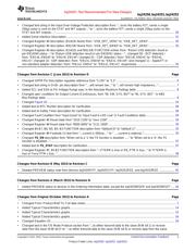
Changes from Revision C (June 2013) to Revision D Page
• Changed VDPM Pin Description regulator reference from "1.23V" to "1.2" .......................................................................... 6
• Changed text string in D+/D- pin description from "....will remain low..." to "...will remain high impedance..."...................... 7
• Added SCL and SDA to Pin Voltage Range spec in the Absolute Maximum Ratings table.................................................. 8
• Changed spec conditions for Output Current (Continuous), from "IN, SW, SYS, BAT" to "IN, SYS, BAT " in ABS
Max Ratings table .................................................................................................................................................................. 8
• Changed Figure 20 .............................................................................................................................................................. 25
• Added text to NTC Monitor description for clarification........................................................................................................ 28
• Added text to Safety Timer description for clarification........................................................................................................ 28
• Changed Fault Condition from "Input Good" to "Input Fault & LDO Low" in Fault Conditions table.................................... 29
• Changed Register #2 Reset state from "1010 1100" to "xxxx 1100" ................................................................................... 34
• Changed Register #4 Reset state from "0000 0000" to "1111 1000"................................................................................... 35
• Changed Bit B7, B6, B5, B4, B3 FUNCTION description from "(default 0)" to "(default 1)" ................................................ 35
• Changed Register #4 Footnote (1) text from "...current is 500ma...." to " .....current is external.."...................................... 35
• Changed TS_EN description from "When set to a ‘1' the TS function is disabled ....." to "When set to a ‘0’, the TS
function is disabled..."........................................................................................................................................................... 37
• Added text to TS_STAT description for clarification............................................................................................................. 37
• Changed Register #7, Bit B3 FUNCTION description from "...if TERM is true or EN_PTM is true..." to "if TERM is
true or Force PTM s true...".................................................................................................................................................. 38
Changes from Revision B (May 2013) to Revision C Page
• Deleted PREVIEW status note from devices bq24250YFF, bq24251YFF, bq24251RGE, and bq24253RGE ................... 45
Changes from Revision A (March 2013) to Revision B Page
• Added PREVIEW status to devices in the Ordering Information table, except the bq24250RGER and bq24250RGET .... 45
Changes from Original (October 2012) to Revision A Page
• Changed From: Product Brief To: Full data sheet.................................................................................................................. 1
• Added Typical Characteristics graphs.................................................................................................................................. 14
• Added Typical Characteristics graphs.................................................................................................................................. 15
• Added Typical Characteristics graphs.................................................................................................................................. 16
• Changed Equation (3) .......................................................................................................................................................... 20
• Changed text in the F/S Mode Protocol section from "...to either transmit data to the slave (R/W bit 1) or receive
data from the slave (R/W bit 0" to "...to either transmit data to the slave (R/W bit 0) or receive data from the slave
Copyright © 2012–2015, Texas Instruments Incorporated Submit Documentation Feedback 3
Product Folder Links: bq24250 bq24251 bq24253
bq24251: Not Recommended For New Designs
器件 Datasheet 文档搜索
AiEMA 数据库涵盖高达 72,405,303 个元件的数据手册,每天更新 5,000 多个 PDF 文件
