Datasheet 搜索 > 电池管理芯片 > TI(德州仪器) > BQ24250YFFR 数据手册 > BQ24250YFFR 数据手册 7/58 页
 器件3D模型
¥ 16.956
BQ24250YFFR 数据手册 - TI(德州仪器)
制造商:
TI(德州仪器)
分类:
电池管理芯片
封装:
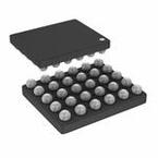
UFBGA-30
描述:
2A单输入I2C ,独立开关模式锂离子电池充电器与电源路径管理 2A Single Input I2C, Standalone Switch-Mode Li-Ion Battery Charger with Power-Path Management
Pictures:
3D模型
符号图
焊盘图
引脚图
产品图
页面导航:
引脚图在P6P7P8Hot
典型应用电路图在P40P41
原理图在P18
封装尺寸在P48P50P51P55
焊盘布局在P56
标记信息在P48P49
封装信息在P9P46P48P49P50P51
技术参数、封装参数在P9
应用领域在P1P58
电气规格在P10P11P12P13P14
导航目录
BQ24250YFFR数据手册
Page:
of 58 Go
若手册格式错乱,请下载阅览PDF原文件
bq24250
,
bq24251
,
bq24253
www.ti.com
SLUSBA1H –OCTOBER 2012–REVISED AUGUST 2015
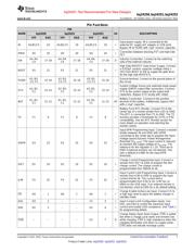
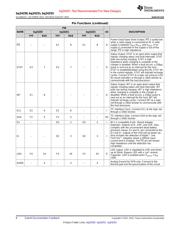
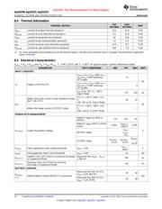
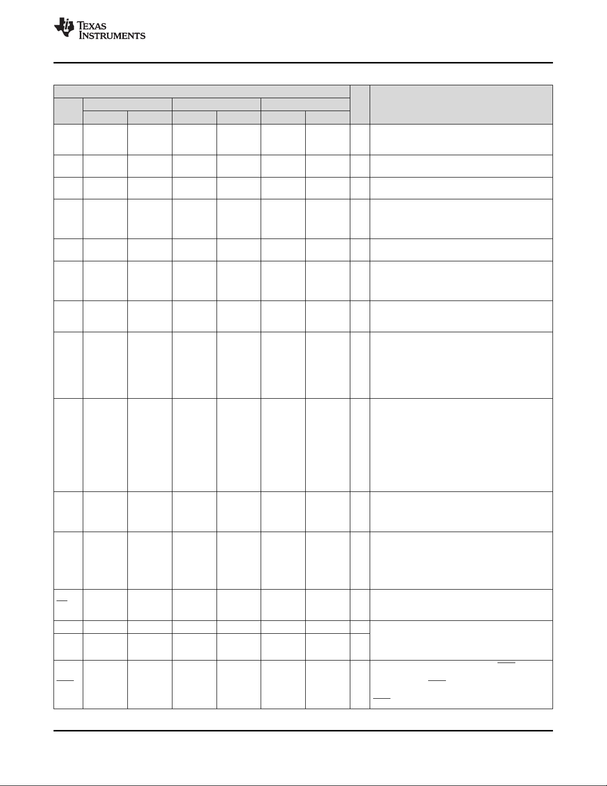
Pin Functions
PIN
NAME bq24250 bq24251 bq24253 I/O DESCRIPTION
YFF RGE YFF RGE YFF RGE
Input power supply. IN is connected to the
IN A5,B5,C5 19 A5,B5,C5 19 A5,B5,C5 19 I external DC supply (AC adapter or USB port).
Bypass IN to PGND with >2μF ceramic capacitor
Connection between blocking FET and high-side
PMID D5 20 D5 20 D5 20 I
FET.
A4, B4, A4, B4, A4, B4, Inductor Connection. Connect to the switching
SW 17–18 17–18 17–18 O
C4 C4 C4 side of the external inductor.
High Side MOSFET Gate Driver Supply. Connect
a 0.033μF ceramic capacitor (voltage rating >
BOOT E5 21 E5 21 E5 21 I
15V) from BOOT to SW to supply the gate drive
for the high side MOSFETs.
A3, B3, A3, B3, A3, B3, Ground terminal. Connect to the ground plane of
PGND 15–16 15–16 15–16
C3, F3 C3, F3 C3, F3 the circuit.
System Voltage Sense and switched-mode power
A2, B2, A2, B2, A2, B2, supply (SMPS) output filter connection. Connect
SYS 13–14 13–14 13–14 I
C2 C2 C2 SYS to the system output at the output bulk
capacitors. Bypass SYS locally with >20μF.
Battery Connection. Connect to the positive
A1, B1, A1, B1, A1, B1,
BAT 11–12 11–12 11–12 I/O terminal of the battery. Additionally, bypass BAT
C1 C1 C1
with a >1μF capacitor.
Battery Pack NTC Monitor. Connect TS to the
center tap of a resistor divider from LDO to GND.
The NTC is connected from TS to GND. The TS
TS F1 9 F1 9 F1 9 I function provides 4 thresholds for JEITA or PSE
compatibility. See the NTC Monitor section for
more details on operation and selecting the
resistor values.
Input DPM Programming Input. Connect a resistor
divider between IN and GND with VDPM
connected to the center tap to program the Input
Voltage based Dynamic Power Management
threshold (V
IN_DPM
). The input current is reduced
VDPM E4 23 E4 23 E4 23 I
to maintain the supply voltage at V
IN_DPM
. The
reference for the regulator is 1.2V. Short pin to
GND if external resistors are not desired—this
sets a default of 4.68V for the input DPM
threshold.
Charge Current Programming Input. Connect a
resistor from ISET to GND to program the fast
ISET D1 10 D1 10 D1 10 I
charge current. The charge current is
programmable from 300mA to 2A.
Input Current Limit Programming Input. Connect a
resistor from ILIM to GND to program the input
current limit for IN. The current limit is
ILIM F5 22 F5 22 F5 22 I
programmable from 0.5A to 2A. ILIM has no
effect on the USB input. If an external resistor is
not desired, short to GND for a 2A default setting.
Charge Enable Active-Low Input. Connect CE to
CE D4 1 D4 1 D4 1 I a high logic level to place the battery charger in
standby mode.
EN1 D3 2 – – F2 5 I Input Current Limit Configuration Inputs. Use
EN1, and EN2 to control the maximum input
current and enable USB compliance. See Table 1
EN2 D2 3 – – E2 6 I
for programming details.
Charge Status Open Drain Output. CHG is pulled
low when a charge cycle starts and remains low
CHG – – – – E3 7 O while charging. CHG is high impedance when the
charging terminates and when no supply exists.
CHG does not indicate recharge cycles.
Copyright © 2012–2015, Texas Instruments Incorporated Submit Documentation Feedback 7
Product Folder Links: bq24250 bq24251 bq24253
bq24251: Not Recommended For New Designs
器件 Datasheet 文档搜索
AiEMA 数据库涵盖高达 72,405,303 个元件的数据手册,每天更新 5,000 多个 PDF 文件
