Datasheet 搜索 > 微控制器 > Silicon Labs(芯科) > C8051F060-GQ 数据手册 > C8051F060-GQ 数据手册 39/329 页
 器件3D模型
¥ 193.714
C8051F060-GQ 数据手册 - Silicon Labs(芯科)
制造商:
Silicon Labs(芯科)
分类:
微控制器
封装:
TQFP-100
描述:
C8051F0xx 微控制器,Silicon Labs25 MIPS 8051 CPU 32 至 64 KB 闪存 256 至 4352 B RAM 2 12 位 DAC 温度传感器 5 或 6 PCA 通道 ### 8051 微控制器,Silicon Labs
Pictures:
3D模型
符号图
焊盘图
引脚图
产品图
页面导航:
引脚图在P39P40P41P42P43P44P117P205P208P327Hot
典型应用电路图在P328
原理图在P21P22P23P24P30P33P35P36P53P67P75P87
封装尺寸在P47P50P327
技术参数、封装参数在P37P74P101P203
应用领域在P166
电气规格在P38P73P74P101P109P112P114P116P119P122P164P169
型号编号列表在P37
导航目录
C8051F060-GQ数据手册
Page:
of 329 Go
若手册格式错乱,请下载阅览PDF原文件
C8051F060/1/2/3/4/5/6/7
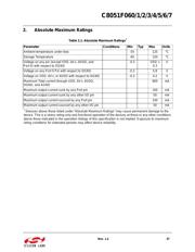
Rev. 1.2 39
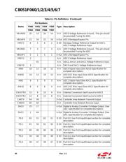
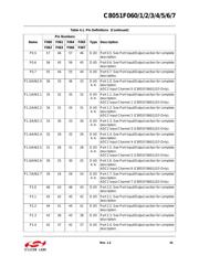
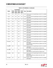
4. Pinout and Package Definitions
Table 4.1. Pin Definitions
Name
Pin Numbers
Type DescriptionF060 F061 F064 F065
F062 F063 F066 F067
VDD 37, 64,
90
26, 40,
55
37, 64,
90
26, 40,
55
Digital Supply Voltage. Must be tied to +2.7 to
+3.6 V.
DGND 38, 63,
89
27, 39,
54
38, 63,
89
27, 39,
54
Digital Ground. Must be tied to Ground.
AV+ 11, 16,
24
7, 10,
18
11, 16,
24
7, 10,
18
Analog Supply Voltage. Must be tied to +2.7 to
+3.6 V.
AVDD 13 23 13 23 Analog Supply Voltage. Must be tied to +2.7 to
+3.6 V.
AGND 10, 14,
17, 23
6, 11,
19, 22
10, 14,
17, 23
6, 11,
19, 22
Analog Ground. Must be tied to Ground.
TMS 96 52 96 52 D In JTAG Test Mode Select with internal pull-up.
TCK 97 53 97 53 D In JTAG Test Clock with internal pull-up.
TDI 98 56 98 56 D In JTAG Test Data Input with internal pull-up. TDI is
latched on the rising edge of TCK.
TDO 99 57 99 57 D Out JTAG Test Data Output with internal pull-up. Data is
shifted out on TDO on the falling edge of TCK. TDO
output is a tri-state driver.
/RST 100 58 100 58 D I/O Device Reset. Open-drain output of internal VDD
monitor. Is driven low when VDD is <2.7 V and
MONEN is high. An external source can initiate a
system reset by driving this pin low.
XTAL1 26 20 26 20 A In Crystal Input. This pin is the return for the internal
oscillator circuit for a crystal or ceramic resonator.
For a precision internal clock, connect a crystal or
ceramic resonator from XTAL1 to XTAL2. If over-
driven by an external CMOS clock, this becomes
the system clock.
XTAL2 27 21 27 21 A Out Crystal Output. This pin is the excitation driver for a
crystal or ceramic resonator.
MONEN 28 63 28 63 D In VDD Monitor Enable. When tied high, this pin
enables the internal VDD monitor, which forces a
system reset when VDD is < 2.7 V. When tied low,
the internal VDD monitor is disabled. Recom-
mended configuration is to connect directly to VDD.
VREF 4 61 4 61 A Out Bandgap Voltage Reference Output
VREF0 21 15 21 15 A I/O Bandgap Voltage Reference Output for ADC0.
ADC0 Voltage Reference Input.
器件 Datasheet 文档搜索
AiEMA 数据库涵盖高达 72,405,303 个元件的数据手册,每天更新 5,000 多个 PDF 文件
