Datasheet 搜索 > 微控制器 > Silicon Labs(芯科) > C8051F310-GQR 数据手册 > C8051F310-GQR 数据手册 67/228 页
 器件3D模型
¥ 14.567
C8051F310-GQR 数据手册 - Silicon Labs(芯科)
制造商:
Silicon Labs(芯科)
分类:
微控制器
封装:
LQFP-32
描述:
C8051F310-GQR 编带
Pictures:
3D模型
符号图
焊盘图
引脚图
产品图
页面导航:
引脚图在P39P40Hot
典型应用电路图在P228
原理图在P19P20P21P22P23P24P25P26P32P33P34P51
封装尺寸在P42P44P48
型号编码规则在P18
标记信息在P221
技术参数、封装参数在P35P65P115P129
电气规格在P36P37P38P65P68P78P110P112P121P123P129P143
型号编号列表在P35P115
导航目录
C8051F310-GQR数据手册
Page:
of 228 Go
若手册格式错乱,请下载阅览PDF原文件
C8051F310/1/2/3/4/5/6/7
Rev. 1.7 67
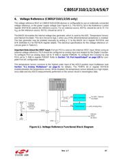
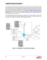
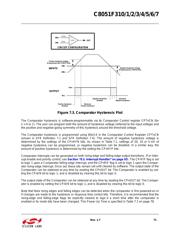
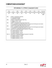
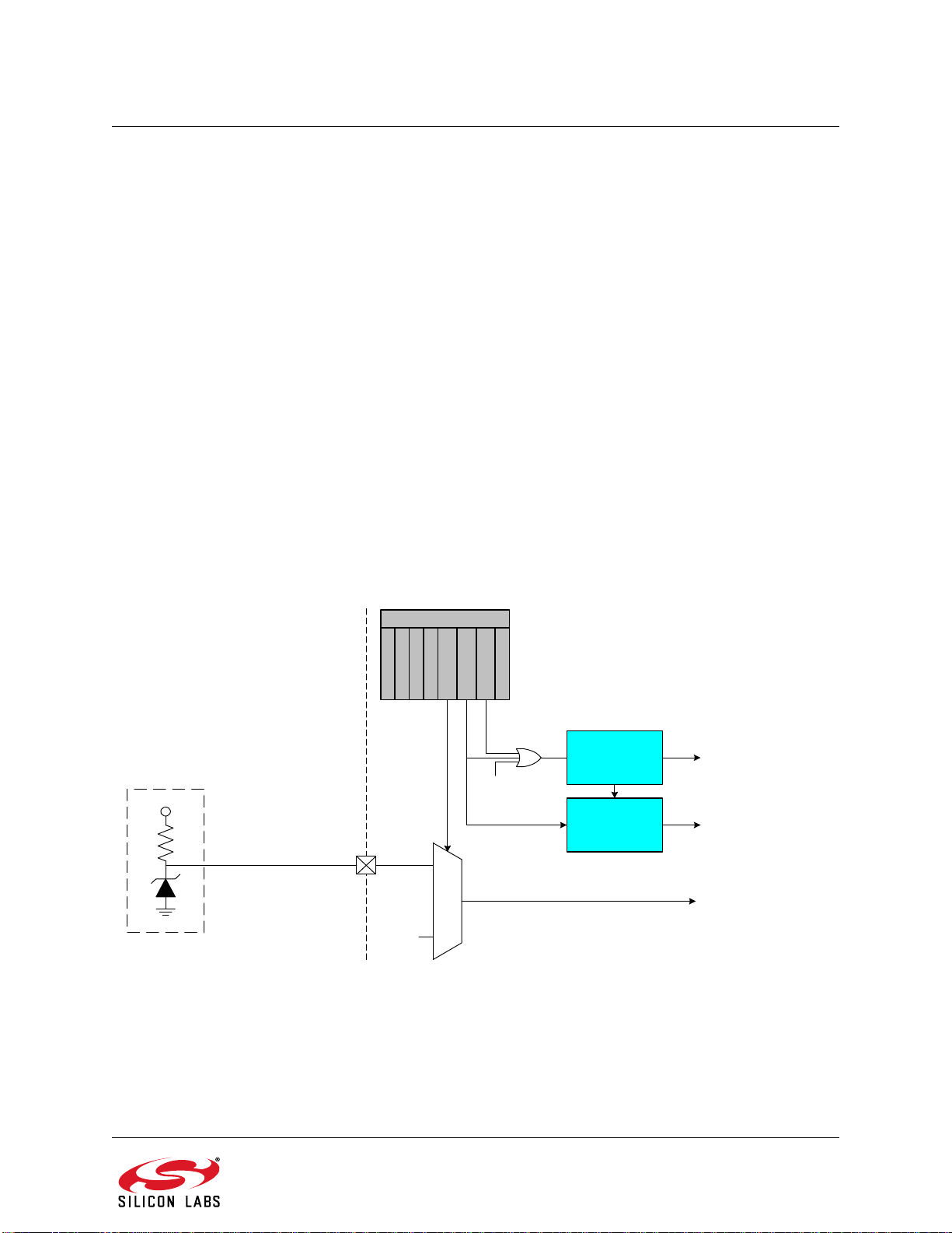
6. Voltage Reference (C8051F310/1/2/3/6 only)
The voltage reference MUX on C8051F310/1/2/3/6 devices is configurable to use an externally connected
voltage reference, or the power supply voltage (see Figure 6.1). The REFSL bit in the Reference Control
register (REF0CN) selects the reference source. For an external source, REFSL should be set to ‘0’; For
V
DD
as the reference source, REFSL should be set to ‘1’.
The BIASE bit enables the internal vol
tage bias generator, which is used by the ADC, Temperature Sensor,
and Internal Oscillator. This bit is forced to logic 1 when any of the aforementioned peripherals is enabled.
The bias generator may be enabled manually by writing a ‘1’ to the BIASE bit in register REF0CN; see
SFR Definition 6.1 for REF0CN register details. The electrical sp
ecifications for the voltage reference cir-
cuit are given in Table 6.1.
Important Note About the VREF Input: Por
t pin P0.0 is used as the external VREF input. When using an
external voltage reference, P0.0 should be configured as analog input and skipped by the Digital Crossbar.
To configure P0.0 as analog input, set to ‘0’ Bit0 in register P0MDIN. To configure the Crossbar to skip
P0.0, set to ‘1’ Bit0 in register P0SKIP. Refer to Section “13. Port Input/Output” on page 129 for com-
plete Port I/O configuration details.
The temperature sensor connects to the highest order input of the ADC0 positive input multiplexer (see
Section “5.1. Analog Multiplexer” on page 51 for details). The TEMPE bit in register REF0CN
enables/disables the temperature sensor. While disabled
, the temperature sensor defaults to a high imped-
ance state and any ADC0 measurements performed on the sensor result in meaningless data.
Figure 6.1. Voltage Reference Functional Block Diagram
Internal
VREF
(to ADC)
To Analog Mux
VDD
VREF
R1
VDD
External
Voltage
Reference
Circuit
GND
REF0CN
REFSL
TEMPE
BIASE
Temp Sensor
EN
Bias Generator
To ADC, Internal
Oscillator
EN
IOSCEN
0
1
器件 Datasheet 文档搜索
AiEMA 数据库涵盖高达 72,405,303 个元件的数据手册,每天更新 5,000 多个 PDF 文件
