Datasheet 搜索 > ON Semiconductor(安森美) > CAT6219-285MV2 数据手册 > CAT6219-285MV2 数据手册 2/11 页


¥ 0
CAT6219-285MV2 数据手册 - ON Semiconductor(安森美)
制造商:
ON Semiconductor(安森美)
Pictures:
3D模型
符号图
焊盘图
引脚图
产品图
页面导航:

导航目录
CAT6219-285MV2数据手册
Page:
of 11 Go
若手册格式错乱,请下载阅览PDF原文件
CAT6219
http://onsemi.com
2
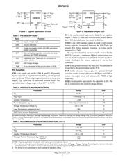
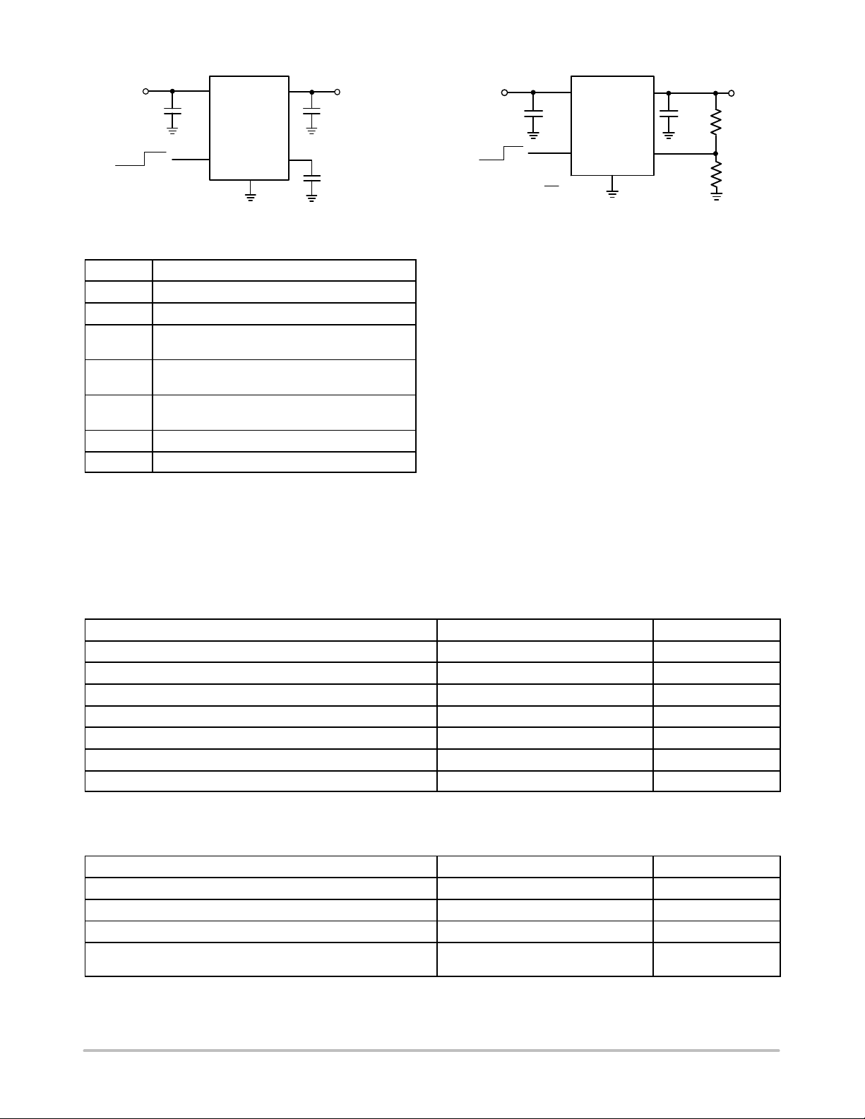
Figure 1. Typical Application Circuit
VIN
BYPEN
VOUT
GND
OFF
ON
1 mF
2.3 V
to 5.5 V
2.2 mF
10 nF
CAT6219
Figure 2. Adjustable Output LDO
C
IN
V
IN
V
OUT
C
OUT
C
BYP
(Optional)
VIN
CAT6219
ADJEN
VOUT
GND
OFF
ON
1 mF
2.3 V
to 5.5 V
2.2 mF
R
1
R
2
C
OUT
V
OUT
V
IN
C
IN
V
OUT
+ 1.24 V
ǒ
1 )
R
1
R
2
Ǔ
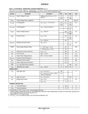
Table 1. PIN DESCRIPTIONS
Name Function
VIN Supply voltage input.
GND Ground reference.
EN
Enable input (active high); a 2.5 MW pull−down
resistor is provided.
BYP Optional bypass capacitor connection for noise
reduction and PSRR enhancing.
ADJ Adjustable input. Feedback pin connected to
resistor divider.
VOUT LDO Output Voltage.
TAB To be connected to the ground plane on PCB
Pin Function
VIN is the supply pin for the LDO. A small 1 mF ceramic
bypass capacitor is required between the V
IN
pin and ground
near the device. When using longer connections to the power
supply, C
IN
value can be increased without limit. The
operating input voltage range is from 2.3 V to 5.5 V.
EN is the enable control logic (active high) for the regulator
output. It has a 2.5 MW pull−down resistor, which assures
that if EN pin is left open, the circuit is disabled.
VOUT is the LDO regulator output. A small 2.2 mF ceramic
bypass capacitor is required between the VOUT pin and
ground. For better transient response, its value can be
increased to 4.7 mF.
The capacitor should be located near the device. For the
SOT23-5 package, a continuous 500 mA output current may
turn-on the thermal protection. A 250 W internal shutdown
switch discharges the output capacitor in the no-load
condition.
GND is the ground reference for the LDO. The pin must be
connected to the ground plane on the PCB.
BYP is the reference bypass pin. An optional 0.01 mF
capacitor can be connected between BYP pin and GND to
reduce the output noise and enhance the PSRR at high
frequency.
ADJ is the adjustable input pin for the adjustable LDO. The
pin is connected to the resistor voltage divider.
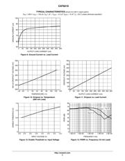
Table 2. ABSOLUTE MAXIMUM RATINGS
Parameter Rating Unit
V
IN
0 to 6.5 V
V
EN
, V
OUT
−0.3 to V
IN
+ 0.3 V
Junction Temperature, T
J
+150
_C
Power Dissipation, P
D
Internally Limited (Note 1) mW
Storage Temperature Range, T
S
−65 to +150
_C
Lead Temperature (soldering, 5 sec.) 260
_C
ESD Rating (Human Body Model) 3 kV
Stresses exceeding Maximum Ratings may damage the device. Maximum Ratings are stress ratings only. Functional operation above the
Recommended Operating Conditions is not implied. Extended exposure to stresses above the Recommended Operating Conditions may affect
device reliability.
Table 3. RECOMMENDED OPERATING CONDITIONS (Note 2)
Parameter Range Unit
V
IN
2.3 to 5.5 V
V
EN
0 to V
IN
V
Junction Temperature Range, T
J
−40 to +125
_C
Package Thermal Resistance, θ
JA
SOT23−5
Package Thermal Resistance, θ
JA
TDFN−6
235
206
_C/W
NOTE: Typical application circuit with external components is shown above.
1. The maximum allowable power dissipation at any T
A
(ambient temperature) is P
Dmax
= (T
Jmax
− T
A
)/q
JA
. Exceeding the maximum allowable
power dissipation will result in excessive die temperature, and the regulator will go into thermal shutdown.
2. The device is not guaranteed to work outside its operating rating.
器件 Datasheet 文档搜索
AiEMA 数据库涵盖高达 72,405,303 个元件的数据手册,每天更新 5,000 多个 PDF 文件
