Datasheet 搜索 > RF射频器件 > TI(德州仪器) > CC2511F32RSPR 数据手册 > CC2511F32RSPR 数据手册 38/245 页
 器件3D模型
¥ 38.183
CC2511F32RSPR 数据手册 - TI(德州仪器)
制造商:
TI(德州仪器)
分类:
RF射频器件
封装:
QFN-36
描述:
低功耗的SoC (系统级芯片)与MCU,存储器, 2.4 GHz射频收发器和USB控制器 Low-Power SoC (System-on-Chip) with MCU, Memory, 2.4 GHz RF Transceiver, and USB Controller
Pictures:
3D模型
符号图
焊盘图
引脚图
产品图
页面导航:
典型应用电路图在P38
原理图在P30P38P137P167P207
封装尺寸在P236P238P239
焊盘布局在P38
标记信息在P236P237
封装信息在P236P237P238P239
焊接温度在P8
功能描述在P1P6
技术参数、封装参数在P8P10
应用领域在P1P245
电气规格在P10
导航目录
CC2511F32RSPR数据手册
Page:
of 245 Go
若手册格式错乱,请下载阅览PDF原文件
CC2510Fx / CC2511Fx
SWRS055G Page 38 of 236
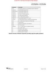
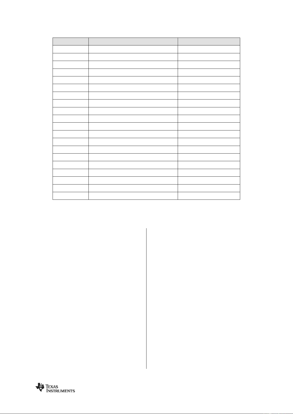
Component Value Manufacturer
C301 1 µF ± 10%, 0402 X5R Murata GRM1555C series
C203/C214 33 pF ± 5%, 0402 NP0 Murata GRM1555C series
C202 56 pF
C212 10 nF
C213 33 pF
C201/C211 27 pF ± 5%, 0402 NP0 Murata GRM1555C series
C231, C241 100 pF ± 5%, 0402 NP0 Murata GRM1555C series
C171, C181 15 pF ± 5%, 0402 NP0 Murata GRM1555C series
C232, C242 1.0 pF ± 0.25 pF, 0402 NP0 Murata GRM1555C series
C233 1.8 pF ± 0.25 pF, 0402 NP0 Murata GRM1555C series
C234 1.5 pF ± 0.25 pF, 0402 NP0 Murata GRM1555C series
L231, L232, L241 1.2 nH ± 0.3 nH, 0402 monolithic Murata LQG-15 series
L281 470 nH ± 10% Murata LQM18NNR47K00
R271 56 kΩ ± 1%, 0402 Koa RK73 series
R264 1.5 kΩ ± 1% Koa RK73 series
R262/R263 33 Ω ± 2% Koa RK73 series
X1 26.0 MHz surface mount crystal NDK, AT-41CD2
X2 32.768 kHz surface mount crystal (optional) Epson MC-306 Crystal Unit
X3 48.0 MHz surface mount crystal (fundamental) Abracon ABM8 series
X4 48.0 MHz surface mount crystal (3
rd
overtone)
Table 29: Bill Of Materials for the CC2510Fx/CC2511Fx Application Circuits (subject to changes)
9.7 PCB Layout Recommendations
The top layer should be used for signal routing,
and the open areas should be filled with
metallization connected to ground using
several vias.
The area under the chip is used for grounding
and shall be connected to the bottom ground
plane with several vias for good thermal
performance and sufficiently low inductance to
ground. In the CC2510EM reference designs
[1] 9 vias are placed inside the exposed die
attached pad. These vias should be “tented”
(covered with solder mask) on the component
side of the PCB to avoid migration of solder
through the vias during the solder reflow
process.
The solder paste coverage should not be
100%. If it is, out gassing may occur during the
reflow process, which may cause defects
(splattering, solder balling). Using “tented” vias
reduces the solder paste coverage below
100%.
See Figure 13 for top solder resist and top
paste masks recommendations.
Each decoupling capacitor should be placed
as close as possible to the supply pin it is
supposed to decouple. The best routing is from
the power line to the decoupling capacitor and
then to the
CC2510Fx
supply pin. Supply power
filtering is very important.
Each decoupling capacitor ground pad should
be connected to the ground plane using a
separate via. Direct connections between
neighboring power pins will increase noise
coupling and should be avoided unless
absolutely necessary.
The external components should ideally be as
small as possible (0402 is recommended) and
surface mount devices are highly
recommended. Please note that components
smaller than those specified may have differing
characteristics.
Schematic, BOM, and layout Gerber files are
all available from the TI website for both the
CC2510EM reference design [1] and the
CC2511 USB Dongle reference design [2].
CC2511F8 - Not Recommended for New Designs
器件 Datasheet 文档搜索
AiEMA 数据库涵盖高达 72,405,303 个元件的数据手册,每天更新 5,000 多个 PDF 文件
