Datasheet 搜索 > 触发器 > TI(德州仪器) > CD4013BPWR 数据手册 > CD4013BPWR 数据手册 1/28 页

 器件3D模型
¥ 0.821
CD4013BPWR 数据手册 - TI(德州仪器)
制造商:
TI(德州仪器)
分类:
触发器
封装:
TSSOP-14
描述:
TEXAS INSTRUMENTS CD4013BPWR 逻辑芯片, D型触发器, 45NS, TSSOP-14
Pictures:
3D模型
符号图
焊盘图
引脚图
产品图
页面导航:
引脚图在P3Hot
典型应用电路图在P1P11P12
原理图在P10
封装尺寸在P15P16P18P19P21
焊盘布局在P13P22
标记信息在P15P16
封装信息在P14P15P16P17P18P19
技术参数、封装参数在P4P11
应用领域在P1P17
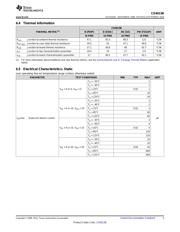
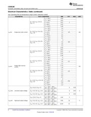
电气规格在P5P6P7P8
导航目录
CD4013BPWR数据手册
Page:
of 28 Go
若手册格式错乱,请下载阅览PDF原文件
CL
V
DD
= Pin 14
V
SS
= Pin 7
V
DD
V
SS
4 (10)
RESET
TG
CL
5 (9)
DATA
p
n
MASTER SECTION
CL
TG
CL
p
n
6 (8)
SET
3 (11)
CL
CL CL
CL
TG
CL
p
n
CL
TG
CL
p
n
1 (13)
Q
Q
SLAVE SECTION
2 (12)
Buffered Outputs
All inputs are protected by
CMOS protection network
Copyright © 2016, Texas Instruments Incorporated
Product
Folder
Sample &
Buy
Technical
Documents
Tools &
Software
Support &
Community
An IMPORTANT NOTICE at the end of this data sheet addresses availability, warranty, changes, use in safety-critical applications,
intellectual property matters and other important disclaimers. PRODUCTION DATA.
CD4013B
SCHS023E –NOVEMBER 1998–REVISED SEPTEMBER 2016
CD4013B CMOS Dual D-Type Flip-Flop
1
1 Features
1
• Asynchronous Set-Reset Capability
• Static Flip-Flop Operation
• Medium-Speed Operation: 16 MHz (Typical) Clock
Toggle Rate at 10-V Supply
• Standardized Symmetrical Output Characteristics
• Maximum Input Current Of 1-µA at 18 V Over Full
Package Temperature Range:
– 100 nA at 18 V and 25°C
• Noise Margin (Over Full Package Temperature
Range):
– 1 V at V
DD
= 5 V
– 2 V at V
DD
= 10 V
– 2.5 V at V
DD
= 15 V
2 Applications
• Power Delivery
• Grid Infrastructure
• Medical, Healthcare, and Fitness
• Body Electronics and Lighting
• Building Automation
• Telecom Infrastructure
• Test and Measurement
3 Description
The CD4013B device consists of two identical,
independent data-type flip-flops. Each flip-flop has
independent data, set, reset, and clock inputs and Q
and Q outputs. These devices can be used for shift
register applications, and, by connecting Q output to
the data input, for counter and toggle applications.
The logic level present at the D input is transferred to
the Q output during the positive-going transition of the
clock pulse. Setting or resetting is independent of the
clock and is accomplished by a high level on the set
or reset line, respectively.
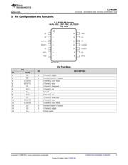
The CD4013B types are supplied in 14-pin dual-in-
line plastic packages (E suffix), 14-pin small-outline
packages (M, MT, M96, and NSR suffixes), and
14-pin thin shrink small-outline packages (PW and
PWR suffixes).
Device Information
(1)
PART NUMBER PACKAGE BODY SIZE (NOM)
CD4013BE PDIP (14) 19.30 mm x 6.35 mm
CD4013BF CDIP (14) 19.50 mm x 6.92 mm
CD4013BM SOIC (14) 8.65 mm x 3.90 mm
CD4013BNS SO (14) 10.20 mm x 5.30 mm
CD4013BPW TSSOP (14) 5.00 mm x 4.40 mm
(1) For all available packages, see the orderable addendum at
the end of the data sheet.
Logic Diagram
器件 Datasheet 文档搜索
AiEMA 数据库涵盖高达 72,405,303 个元件的数据手册,每天更新 5,000 多个 PDF 文件
