Datasheet 搜索 > Intersil(英特矽尔) > CD4021 数据手册 > CD4021 数据手册 1/9 页


¥ 0
CD4021 数据手册 - Intersil(英特矽尔)
制造商:
Intersil(英特矽尔)
描述:
CMOS 8级静态移位寄存器 CMOS 8-Stage Static Shift Registers
Pictures:
3D模型
符号图
焊盘图
引脚图
产品图
页面导航:
典型应用电路图在P1P6P7
焊盘布局在P9
应用领域在P1
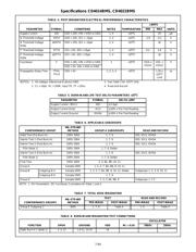
电气规格在P3P4P5P8P9
导航目录
CD4021数据手册
Page:
of 9 Go
若手册格式错乱,请下载阅览PDF原文件
7-80
CAUTION: These devices are sensitive to electrostatic discharge; follow proper IC Handling Procedures.
1-888-INTERSIL or 321-724-7143 | Copyright © Intersil Corporation 1999
CD4014BMS,
CD4021BMS
CMOS 8-Stage Static Shift Registers
Description
CD4014BMS -Synchronous Parallel or Serial Input/Serial Output
CD4021BMS -Asynchronous Parallel Input or Synchronous
Serial Input/Serial Output
CD4014BMS and CD4021BMS series types are 8-stage paral-
lel- or serial-input/serial output registers having common CLOCK
and PARALLEL/SERIAL CONTROL inputs, a single SERIAL
data input, and individual parallel “JAM” inputs to each register
stage. Each register stage is a D-type, master-slave flip-flop. In
addition to an output from stage 8, “Q” outputs are also available
from stages 6 and 7. Parallel as well as serial entry is made into
the register synchronously with the positive clock line transition in
the CD4014BMS. In the CD4021BMS serial entry is synchro-
nous with the clock but parallel entry is asynchronous. In both
types, entry is controlled by the PARALLEL/SERIAL CONTROL
input. When the PARALLEL/SERIAL CONTROL input is low,
data is serially shifted into the 8-stage register synchronously
with the positive transition of the clock line. When the PARALLEL/
SERIAL CONTROL input is high, data is jammed into the 8-
stage register via the parallel input lines and synchronous with
the positive transition of the clock line. In the CD4021BMS, the
CLOCK input of the internal stage is “forced” when asynchro-
nous parallel entry is made. Register expansion using multiple
packages is permitted.
The CD4014BMS and CD4021BMS are supplied in these 16
lead outline packages:
Braze Seal DIP H4T
Frit Seal DIP H1F
Ceramic Flatpack H6W
Features
• High Voltage Types (20V Rating)
• Medium Speed Operation 12MHz (Typ.) Clock Rate at
VDD-VSS = 10V
• Fully Static Operation
• 8 Master-Slave Flip-Flops Plus Output Buffering and
Control Gating
• 100% Tested for Quiescent Current at 20V
• Maximum Input Current of 1µA at 18V Over Full Pack-
age Temperature Range; 100nA at 18V and +25
o
C
• Noise Margin (Full Package Temperature Range)
• 1V at VDD = 5V
• 2V at VDD = 10V
• 2.5V at VDD = 15V
• Standardized Symmetrical Output Characteristics
• 5V, 10V and 15V Parametric Ratings
• Meets All Requirements of JEDEC Tentative Standard
No. 13B, “Standard Specifications for Description of
`B' Series CMOS Devices
Applications:
• Parallel Input/Serial Output Data Queueing
• Parallel to Serial Data Conversion
• General Purpose Register
File Number
3294
December 1992
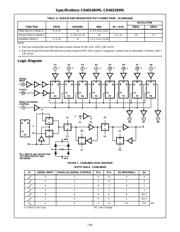
Functional Diagram
14 1513 1456716
12345678
VDD
PAR. IN
VSS
12
3
2
11
10
9
Q6
Q7
Q8
PARALLEL/SERIAL
CONTROL
SERIAL IN
CLOCK
BUFFERED
OUT
8
Pinout
14
15
16
9
13
12
11
10
1
2
3
4
5
7
6
8
PI-8
Q6
Q8
PI-4
PI-3
PI-2
VSS
PI-1
VDD
PI-6
PI-5
Q7
SERIAL IN
CLOCK
PARALLEL/SERIAL
PI-7
CONTROL
器件 Datasheet 文档搜索
AiEMA 数据库涵盖高达 72,405,303 个元件的数据手册,每天更新 5,000 多个 PDF 文件
